
Explore the cutting-edge world of Photonic Bandgap Engineering, its principles, applications, and future in optics innovation and technology.
Understanding Photonic Bandgap Engineering
Photonic Bandgap Engineering is a revolutionary field in optics, offering unprecedented control over light propagation. This domain revolves around manipulating the structure of materials at a microscopic level to create photonic crystals. These crystals have unique properties that allow for the precise control of light, leading to innovative applications in various technological areas.
Principles of Photonic Bandgap Engineering
At the heart of photonic bandgap engineering is the concept of the photonic bandgap (PBG). A PBG is a range of frequencies within which light propagation through a photonic crystal is prohibited. This phenomenon occurs due to the periodic structure of the crystal, which creates a series of interference patterns that can either enhance or inhibit light transmission. By varying the periodic structure, engineers can tailor the photonic bandgap to specific frequencies, thereby controlling the flow of light.
Materials and Fabrication Techniques
The fabrication of photonic crystals is a meticulous process, requiring precision at the nanoscale level. Common materials used include silicon, gallium arsenide, and indium phosphide. These are chosen for their high refractive index contrast, which is essential for creating a pronounced PBG. Advanced techniques such as electron beam lithography, focused ion beam milling, and holographic lithography are employed to achieve the desired nanostructures.
Applications in Modern Technology
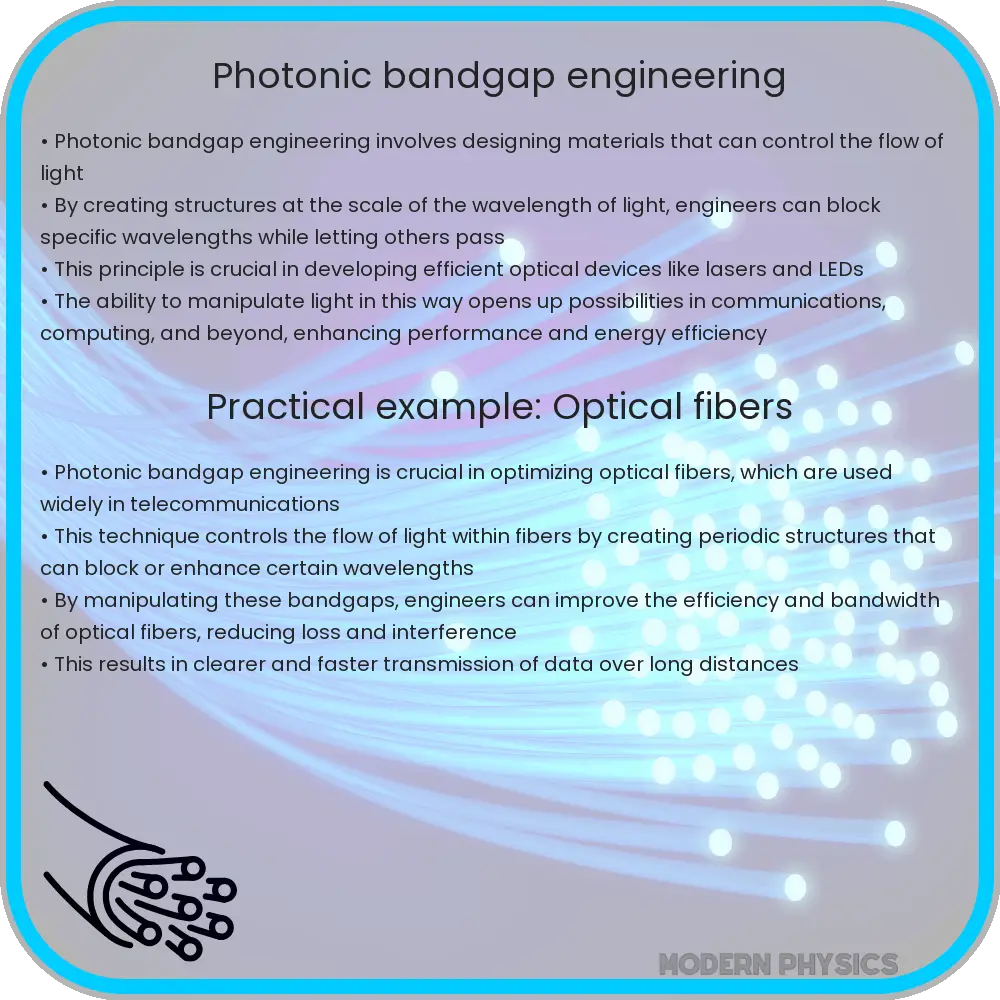
Photonic bandgap engineering has opened the doors to a plethora of applications. One of the most notable is in the development of highly efficient optical fibers, where PBGs are used to confine light with minimal losses. Additionally, PBGs play a crucial role in creating compact and highly selective optical filters, essential in telecommunications for wavelength division multiplexing (WDM). Furthermore, this technology is pivotal in developing new types of lasers, sensors, and even quantum computing components, where control over light at the quantum level is paramount.
With its ability to manipulate light in unprecedented ways, photonic bandgap engineering stands at the forefront of optical innovation. Its continued development promises to revolutionize the field of optics, bringing new capabilities and efficiencies to various technological domains.
Advancements in Photonic Bandgap Research
Recent advancements in photonic bandgap engineering have further expanded its potential. Researchers are exploring the use of novel materials like photonic liquid crystals and metamaterials. These materials offer dynamic control over the photonic bandgap, enabling tunability in real-time which is crucial for adaptive optics systems. Additionally, the integration of photonic crystals with other nanoscale structures has led to the development of superlenses and hyperbolic metamaterials, providing unprecedented resolution beyond the diffraction limit of light.
Challenges and Future Prospects
Despite its promising potential, photonic bandgap engineering faces significant challenges. One of the primary issues is the complexity of fabricating three-dimensional photonic crystals with the required precision at a large scale. There’s also the challenge of integrating these materials with existing optical systems and electronic components. However, ongoing research is addressing these issues, focusing on developing more cost-effective and scalable fabrication methods and exploring hybrid systems that combine photonic crystals with conventional optical materials.
Environmental Impact and Sustainability
An important aspect of photonic bandgap engineering is its environmental impact. The use of non-toxic materials and energy-efficient fabrication processes is gaining attention, aiming to make this technology sustainable and environmentally friendly. Moreover, the energy efficiency of devices utilizing photonic bandgap structures, such as LEDs and solar cells, contributes positively to reducing the carbon footprint in the technology sector.
Conclusion
In conclusion, photonic bandgap engineering represents a significant leap forward in the field of optics. Its ability to precisely control and manipulate light at the nanoscale opens up a world of possibilities, from advanced telecommunications to breakthroughs in quantum computing. While challenges in fabrication and integration remain, the ongoing research and development in this field are paving the way for more efficient, sustainable, and groundbreaking optical technologies. As we continue to explore the potentials of manipulating light at such a fundamental level, photonic bandgap engineering stands as a testament to human ingenuity and the endless pursuit of technological advancement.