
Explore the world of Helium Ion Microscopy: a revolutionary tool for high-resolution imaging, surface analysis, and insights into plasma physics in nanotechnology.
Introduction to Helium Ion Microscopy
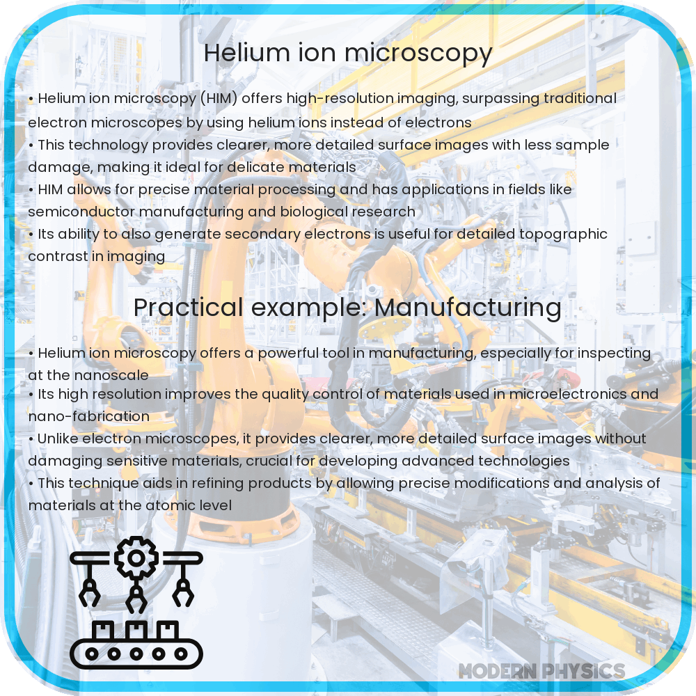
Helium Ion Microscopy (HIM) represents a cutting-edge imaging technology that has dramatically expanded the frontiers of surface analysis and nanotechnology. By utilizing a focused beam of helium ions, HIM offers unparalleled high-resolution imaging and surface characterization capabilities. This technology not only provides images with higher resolution than traditional scanning electron microscopy (SEM) but also delivers comprehensive insights into the material properties at the nanoscale.
Principles of Helium Ion Microscopy
At the core of HIM technology is the generation and manipulation of a focused beam of helium ions (He+). This beam, when directed onto a sample, interacts with the sample’s surface atoms, leading to the emission of secondary electrons. These electrons are then collected to form an image that reveals the topography and composition of the surface at nanometer or even sub-nanometer resolution. The precise control over the helium ion beam allows for detailed surface analysis, making HIM an invaluable tool in materials science, biology, and nanotechnology.
High-Resolution Imaging Capabilities
HIM stands out for its exceptional high-resolution imaging capabilities. It can achieve resolutions of less than 0.5 nm, significantly surpassing the capabilities of SEM. This level of detail enables scientists and researchers to observe and analyze features on the surface of materials that were previously invisible. From the intricate patterns on semiconductor devices to the detailed structures of biological specimens, HIM provides a window into the microscopic world like never before.
Surface Analysis and Material Characterization
Beyond imaging, HIM is also adept at conducting detailed surface analysis and material characterization. It can determine the distribution of chemical elements on a sample’s surface by detecting the characteristic energy levels of the emitted secondary electrons. This capability is crucial for understanding the chemical composition and properties of materials at the nanoscale, leading to advancements in nanotechnology, electronics, and materials science.
Advancements in Plasma Physics
The use of helium ions introduces unique interactions with materials, contributing to the field of plasma physics. The ionization and excitation of atoms at the surface under the helium ion beam provide valuable data on plasma-material interactions, surface dynamics, and ion-induced surface modification processes. These insights are essential for developing new materials and technologies, including semiconductor devices and nanofabrication techniques.
Applications in Research and Industry
Helium Ion Microscopy has found a wide array of applications across various fields due to its superior imaging and analysis capabilities. In the realm of life sciences, HIM allows for the imaging of biological specimens with unprecedented clarity, aiding in cellular and molecular biology research. In materials science, it facilitates the investigation of nanomaterials, polymers, and composites, providing critical insights into their structure and properties. Furthermore, in the semiconductor industry, HIM is instrumental in the fabrication and analysis of microelectronic components, enabling the development of smaller, more efficient devices.
Challenges and Future Directions
Despite its numerous advantages, Helium Ion Microscopy also faces certain challenges. The primary concern is the potential sample damage caused by the helium ion beam, which can limit its application on sensitive materials. Additionally, the cost and complexity of HIM instruments can be prohibitive for some research facilities. However, ongoing advancements in technology are aimed at overcoming these hurdles, making HIM more accessible and versatile. Future developments are expected to enhance the resolution and efficiency of helium ion microscopes further, broadening their application scope and making them a cornerstone technology in nanoscale research and development.
Conclusion
Helium Ion Microscopy has emerged as a pivotal technology in the field of nanotechnology and surface science, offering unmatched high-resolution imaging and detailed surface analysis capabilities. Its ability to provide deep insights into the material properties at the nanoscale has profound implications for research and development across a spectrum of disciplines, including materials science, biology, and semiconductor manufacturing. As we continue to push the boundaries of nanotechnology, the role of HIM in advancing our understanding of the microscopic world is undeniable. With ongoing advancements aimed at mitigating its limitations, Helium Ion Microscopy is set to play an even more significant role in the future of scientific discovery and technological innovation.