
Tunnel diodes, or Esaki diodes, are quantum mechanical devices known for their high efficiency and speed due to quantum tunneling, ideal for high-frequency applications.
Tunnel Diodes: Quantum Applications, Efficiency & Speed
Tunnel diodes, also known as Esaki diodes, are a type of quantum mechanical device that exhibits interesting electrical characteristics due to the phenomenon known as quantum tunneling. Invented by Leo Esaki in 1957, they are highly efficient and fast, making them valuable in various applications, particularly in high-frequency and high-speed electronics.
Understanding Tunnel Diodes
Tunnel diodes are made from heavily doped semiconductor materials, usually germanium, gallium arsenide, or silicon. The heavy doping levels cause the conduction and valence bands to overlap, enabling electrons to “tunnel” through the diode even at very low voltages. This process is fundamentally different from the behavior of conventional diodes and results in unique current-voltage (I-V) characteristics.
Quantum Tunneling
Quantum tunneling is a quantum mechanical effect where particles move through a barrier that they classically shouldn’t be able to pass. In the case of a tunnel diode, electrons tunnel through the potential barrier created by the p-n junction. This tunneling effect is rapid and occurs even when the applied voltage is lower than the potential barrier, which is a behavior that can be exploited for high-speed and high-frequency applications.
Current-Voltage (I-V) Characteristics
The I-V characteristics of a tunnel diode are distinct from ordinary diodes. The curve shows three regions:
The negative resistance region is particularly useful in oscillators and amplifiers because it allows the device to amplify signals or generate high-frequency oscillations.
Efficiency and Speed
Tunnel diodes are known for their high efficiency and speed. Since tunneling is an extremely fast quantum process, these diodes can operate at frequencies well into the gigahertz (GHz) range. They are also efficient because they require very little power to operate. The result is a device that can switch very quickly between states, making them ideal for high-speed electronics.
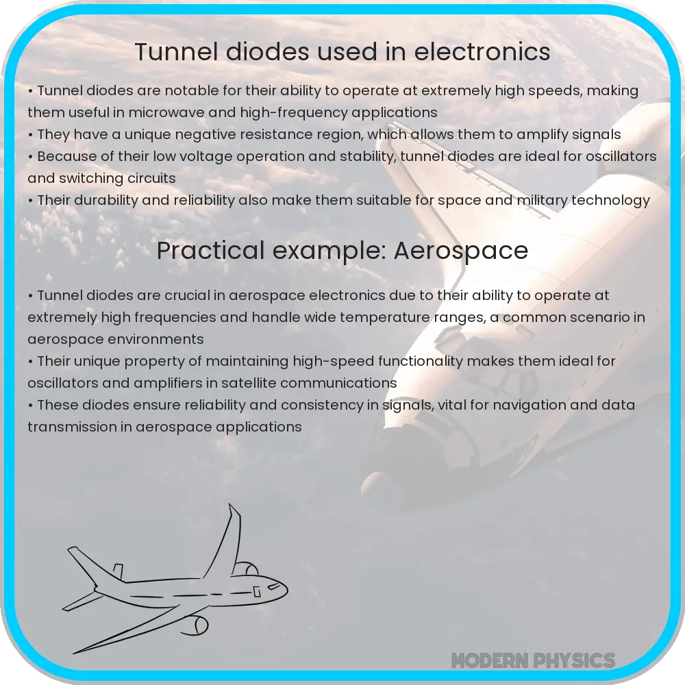
Applications of Tunnel Diodes
Tunnel diodes are utilized in several high-speed and high-frequency electronics applications due to their unique characteristics. Here are a few key applications:
Fabrication of Tunnel Diodes
The manufacturing process of tunnel diodes is critical to their performance. Here’s an overview of the fabrication steps:
Future Prospects of Tunnel Diodes
With the continuous demand for faster and more efficient electronics, tunnel diodes hold a promising future. Researchers are exploring new materials and designs to enhance their performance further:
Conclusion
Tunnel diodes, with their unique quantum tunneling properties, stand as a testament to the fascinating possibilities in the realm of semiconductor devices. Their characteristic I-V curve, featuring a negative resistance region, makes them invaluable in applications requiring high speed and efficiency. From oscillators and amplifiers to switching circuits and memory storage, these diodes have carved out a niche in the electronics industry. As research progresses, the potential to unlock even greater capabilities from tunnel diodes continues to grow, heralding a bright future for quantum-based electronic components.