
Superlattices are engineered materials crafted from layers of different materials, each just a few atoms thick, exhibiting unique physical properties for advanced applications.
Understanding Superlattice Structures
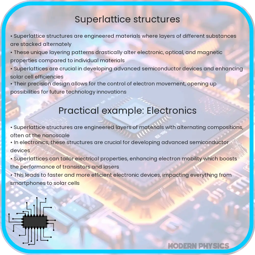
Superlattices are engineered materials made from layers of two or more different materials, each layer often only a few atoms thick. These structures exhibit unique physical properties that are not present in their individual components, making them highly valuable in advanced applications across fields such as electronics, photonics, and materials science.
Design and Fabrication of Superlattices
The design of superlattice structures is a meticulous process that involves choosing appropriate materials based on their lattice constants, electronic properties, and compatibility. This selection aims to create alternating layers with precise thicknesses controlled at the atomic level. The most common methods for fabricating superlattices include molecular beam epitaxy (MBE) and atomic layer deposition (ALD), techniques that allow for high precision and control over the thickness of each layer.
Advanced Uses of Superlattices
Superlattices are at the frontier of many technological advances. Here are some of their most impactful applications:
- Electronics: In electronic devices, superlattices can be used to create highly efficient semiconductors. For instance, the alternating layers can act as quantum wells, confining electrons in a way that enhances mobility, leading to faster and less power-consuming components.
- Photonics: Superlattice structures are employed in the design of photonic devices like laser diodes and detectors. By adjusting the layer thickness, photon interaction can be finely controlled, enabling devices that are highly sensitive and specific for certain wavelengths.
- Thermoelectrics: In thermoelectric materials, superlattices can reduce thermal conductivity while maintaining electrical conductivity. This combination is crucial for efficient energy conversion from waste heat into electricity.
Benefits of Superlattices
Superlattices offer several substantial benefits over traditional materials:
- Enhanced Properties: By combining materials in a superlattice, it’s possible to engineer properties that are not achievable in homogeneous materials. These enhanced properties include greater electrical conductivity, photon control, and thermal management.
- Tailored Band Gaps: Electronic band gaps can be precisely controlled in superlattices, allowing for the design of materials that fit specific needs. This is particularly valuable in semiconductors and photonic devices, where band gap engineering can lead to improvements in efficiency and performance.
- Reduced Defect Density: The process of layering different materials can help to counteract the defects typically present in bulk materials. This reduction in defect density results in higher-quality materials with superior performance.
These attributes of superlattices highlight their potential in revolutionizing fields that rely on precise material characteristics. Continuing research and development are poised to expand their applications and make these advanced materials more accessible and economically viable.
Challenges in Superlattice Development
Despite their promising attributes, the development of superlattices also faces several challenges:
- Complex Fabrication: The sophisticated techniques required for superlattice fabrication, such as MBE and ALD, demand high precision and control. These processes are not only resource-intensive but also require significant expertise, limiting their use to specialized laboratories.
- Material Compatibility: Finding materials that can be effectively layered without causing structural or chemical incompatibilities poses a considerable challenge. These incompatibilities can adversely affect the physical properties and stability of the superlattice.
- Cost: Due to the intricate and careful processing required, producing superlattices is often expensive. Scaling up production while maintaining quality and performance is a major hurdle for the widespread adoption of superlattice technologies.
Future Prospects of Superlattice Technologies
Despite the existing challenges, the future of superlattice technologies is vibrant with opportunities. Ongoing advancements in nanotechnology and materials science continue to push the boundaries of what is possible with superlattices. Researchers are exploring novel ways to simplify fabrication processes and reduce costs, making these materials more accessible for a broader range of applications. Innovations such as the use of two-dimensional materials and nanoparticles within superlattice structures are promising steps toward more practical and versatile applications.
The continued exploration and understanding of superlattice physics also hold the key to unlocking new applications in areas as diverse as renewable energy, sensors, and even quantum computing. As technologies evolve, so too will the capabilities of superlattices to contribute to cutting-edge scientific and industrial developments.
Conclusion
Superlattices represent a fascinating frontier in materials science, providing us with a fine control over material properties that was unimaginable a few decades ago. These engineered materials open up a world of possibilities in electronics, photonics, and thermoelectrics, among other fields, offering significant advantages over traditional materials in terms of performance, energy efficiency, and customizability. Despite the challenges associated with their development, including complex fabrication processes and high costs, researchers are making meaningful progress. With continued investment in innovation and a deepening understanding of their potential, superlattices are poised to play a crucial role in the next generation of technological advancements. By harnessing the unique properties of superlattices, science and engineering can provide solutions to some of the most pressing challenges facing modern society.