
Explore the revolutionary world of quantum plasmonic devices, blending quantum mechanics with nanotechnology for faster, precise, integrated tech.
Exploring the Frontier of Quantum Plasmonic Devices
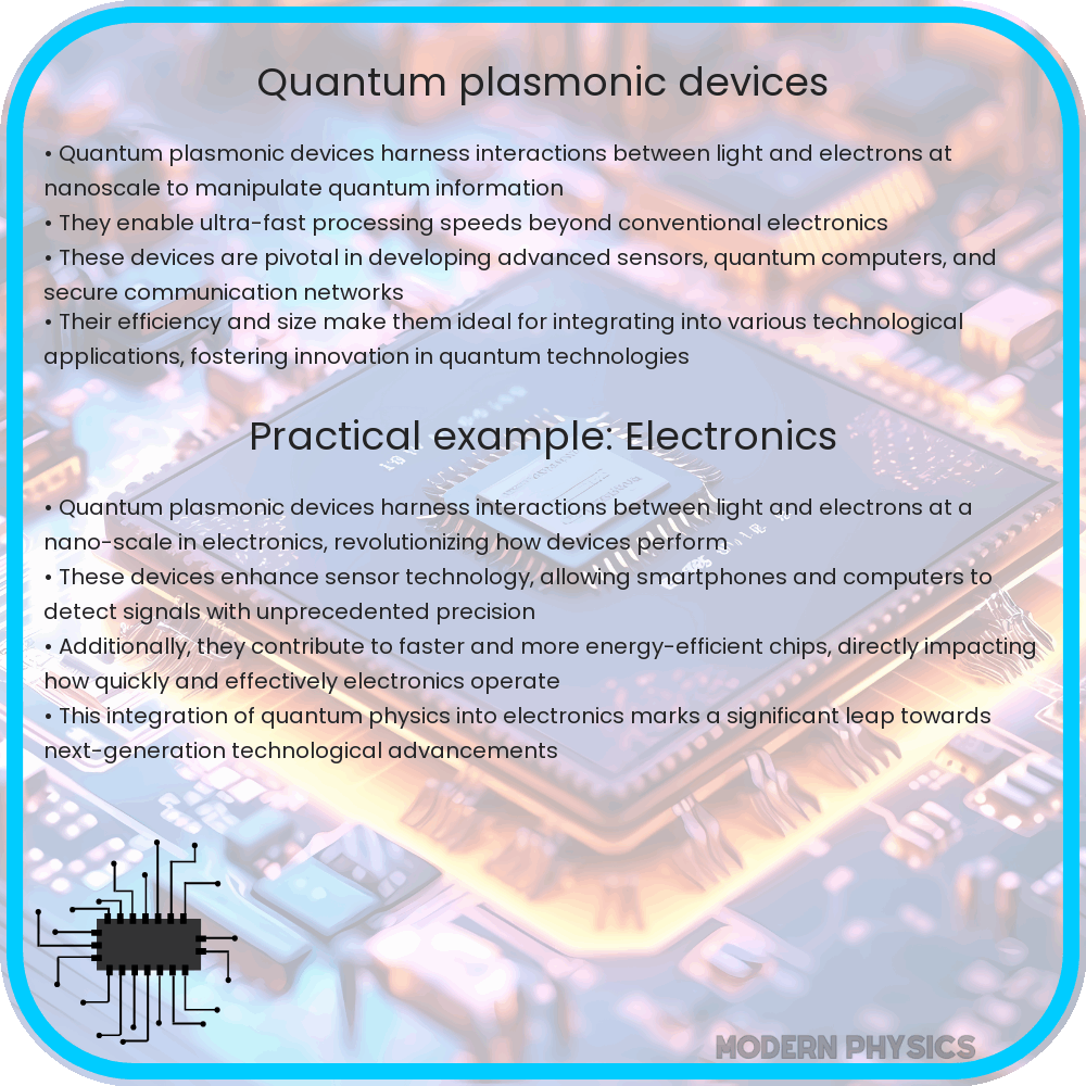
The realm of quantum plasmonics represents a thrilling frontier in nanotechnology, blending the principles of quantum mechanics with plasmonics to forge devices of unprecedented precision, speed, and integration capabilities. At the heart of this innovative field are quantum plasmonic devices (QPDs), which promise to revolutionize various sectors including telecommunications, computing, and sensing technologies.
Understanding Quantum Plasmonics
Quantum plasmonics leverages the quantum effects of electrons on metal surfaces to manipulate light at scales far below the diffraction limit. This is achieved through the excitation of plasmons—quasi-particles resulting from the oscillation of free electrons in response to electromagnetic waves. QPDs exploit these interactions, enabling ultra-compact and fast-operating devices that can outperform traditional optical components in both size and efficiency.
The Promise of Precision and Speed
The precision of QPDs stems from their ability to control light at the nanoscale, allowing for the manipulation of photons with extraordinary accuracy. This capability is essential for the development of advanced sensors and for enhancing the resolution of imaging techniques beyond the capabilities of classical optics. Moreover, the speed at which QPDs operate—often in the terahertz frequency range—opens new avenues for data transmission and processing, potentially overcoming the bandwidth limitations faced by current technologies.
Towards Seamless Integration
One of the most compelling advantages of quantum plasmonic devices is their integrability with existing semiconductor technologies. This compatibility facilitates the creation of hybrid systems that combine the best of quantum and classical technologies, offering a pathway to more powerful and efficient computing architectures. By integrating QPDs with silicon-based electronics, researchers aim to develop quantum circuits that can operate at room temperature, a critical step towards practical quantum computing.
The application of quantum plasmonics in creating QPDs represents a significant leap towards harnessing the full potential of light and quantum mechanics. As research progresses, the promise of these devices in transforming technology as we know it becomes increasingly tangible, heralding a new era of miniaturized, high-speed, and integrated devices.
Advancements and Challenges in Quantum Plasmonic Devices
Despite the promising potential of quantum plasmonic devices, the path to widespread application is fraught with scientific and engineering challenges. One of the foremost issues is the inherent loss of energy that occurs when light interacts with metals, leading to a decrease in the efficiency of these devices. Researchers are actively exploring materials with lower loss rates and innovative device architectures to mitigate these effects. Another challenge is the precise fabrication of nanostructures required for QPDs, which demands advanced manufacturing techniques that can achieve the necessary resolution and accuracy.
Current Applications and Future Directions
Currently, quantum plasmonic devices are making significant impacts in fields such as photovoltaics, where they enhance light absorption in solar cells, and in medical diagnostics, through the development of highly sensitive biosensors. Looking ahead, the potential applications of QPDs are vast and varied. In the realm of information technology, they are poised to play a crucial role in the development of quantum computing and ultra-fast data processing systems. Furthermore, their ability to control light at the nanoscale holds promise for revolutionary advances in imaging and microscopy, potentially enabling scientists to observe phenomena at the quantum level.
Conclusion
The exploration of quantum plasmonic devices is at the cutting edge of nanotechnology and quantum physics, offering a glimpse into a future where the manipulation of light and quantum effects can be harnessed for groundbreaking technological advances. While challenges remain in overcoming the limitations of these devices, the ongoing research and development efforts are paving the way for their integration into a wide range of applications, from enhanced computing capabilities to improved diagnostic tools. As we continue to unlock the mysteries of quantum plasmonics, the potential for innovation is boundless, promising to usher in a new era of technology that is faster, more precise, and more integrated than ever before.