
Explore the revolutionary impact of plasmonic materials in nanophotonics, enhancing light manipulation for applications in sensing, photovoltaics, and optical computing.
Understanding Plasmonic Materials and Their Role in Enhanced Light Manipulation
Plasmonic materials have revolutionized the field of nanophotonics by harnessing the power of light at the nanoscale. These materials consist of metals such as gold (Au), silver (Ag), and aluminum (Al) which exhibit unique properties when exposed to light. This is due to their free electrons that resonate with light waves, leading to enhanced electromagnetic fields at the material’s surface. This phenomenon, known as surface plasmon resonance (SPR), is pivotal in the manipulation of light beyond the diffraction limit of traditional optics.
Applications of Plasmonic Materials in Nanophotonics
Plasmonic materials find extensive applications in various fields due to their unique light-enhancing capabilities. One of the most notable applications is in the development of highly sensitive biosensors. By leveraging the sensitivity of SPR to changes in the local refractive index, these sensors can detect biomolecules at incredibly low concentrations, crucial for early disease diagnosis and environmental monitoring.
- Photovoltaics: Plasmonic nanoparticles integrated into solar cells can significantly increase their efficiency by concentrating light into the active regions of the cell, thus enhancing the absorption of sunlight.
- Medical Therapeutics: In hyperthermia therapy, plasmonic nanoparticles are used to target and destroy cancer cells by converting absorbed light into heat, minimizing damage to surrounding healthy tissues.
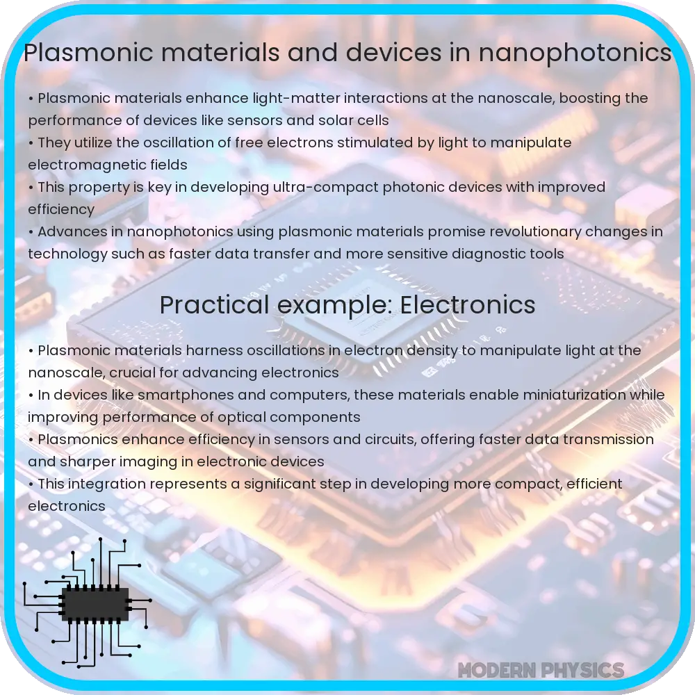
- Optical Computing: Plasmonic materials enable the miniaturization of optical components for data processing at speeds far exceeding current electronic devices, marking a significant step towards faster and more efficient optical computing systems.
The integration of plasmonic materials into nanophotonic devices not only improves performance but also enables new functionalities. For instance, the ability to focus light into nanometer-scale volumes can lead to the development of super-resolution imaging techniques, breaking the barriers of traditional light microscopy.
Innovations in Plasmonic Materials for Advanced Nanophotonic Applications
Recent advancements in nanofabrication techniques have led to the creation of innovative plasmonic structures. These include metamaterials with negative refractive index, enabling superlensing effects, and plasmonic waveguides that allow light to propagate with minimal loss. Additionally, the development of tunable plasmonic materials, whose optical properties can be dynamically adjusted, opens new avenues for reconfigurable photonic devices.
Plasmonic Materials: Pioneers in Nanophotonics
Plasmonic materials have revolutionized the field of nanophotonics by enhancing light-matter interactions at the nanoscale. These materials leverage the unique properties of surface plasmons, which are oscillations of electrons at the interface between a metal and a dielectric. This interaction leads to unprecedented control over light, enabling applications that were previously unattainable.
Applications of Plasmonic Materials
- Sensing: Plasmonic materials are extensively used in biosensing and chemical sensing due to their sensitivity to changes in the local refractive index. This allows for the detection of minute amounts of substances, critical in medical diagnostics and environmental monitoring.
- Photovoltaics: In solar cells, incorporating plasmonic nanoparticles can significantly enhance light absorption and conversion efficiency. They scatter and trap light within the active layers, leading to improved performance.
- Optical Computing: Plasmonic materials facilitate the miniaturization of optical components necessary for optical computing. They can confine light to dimensions below the diffraction limit, enabling the integration of photonic and electronic circuits.
Innovation in Nanophotonics
The innovation brought about by plasmonic materials in nanophotonics is vast and varied. Researchers are exploring new compositions and structures to further enhance the plasmonic effects. For instance, hybrid plasmonic-photonic systems are being developed for better control and manipulation of light. Moreover, advances in fabrication techniques, such as electron beam lithography and nano-imprint lithography, have allowed for the precise and scalable production of plasmonic structures.
Furthermore, the integration of plasmonic materials with other nanostructures like quantum dots and 2D materials is opening new pathways for light manipulation. These combinations lead to hybrid devices capable of ultra-fast data transmission and highly sensitive detection mechanisms, marking a significant step forward in the development of next-generation optical devices.
Conclusion
Plasmonic materials stand at the forefront of nanophotonic innovation, offering a bridge between the macroscopic world of classical optics and the quantum realm. Their ability to control and manipulate light at the nanoscale has opened up new avenues in various applications, from enhanced sensing to more efficient energy harvesting. As research progresses, the potential of these materials continues to expand, promising a future where light can be harnessed in ways we are just beginning to imagine. The synergy between plasmonic materials and nanotechnology marks a pivotal chapter in the advancement of optical technologies, paving the way for a new era of miniaturized, efficient, and highly capable photonic devices.