
Explore the precision, speed, and versatility of plasma etching in semiconductor manufacturing, addressing its mechanism, benefits, challenges, and future outlook.
Introduction to Plasma Etching: Unveiling Its Precision, Speed, and Versatility
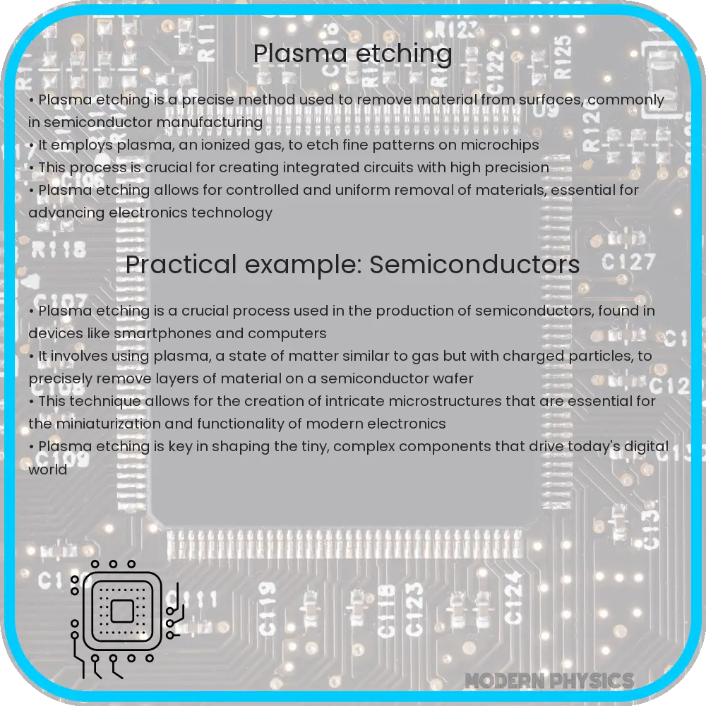
Plasma etching stands as a cornerstone technique in the realm of plasma physics, underpinning various high-precision manufacturing processes, particularly in the semiconductor industry. This advanced method utilizes plasma—a highly ionized gas containing an equal number of positively charged ions and electrons—to selectively remove material from a solid surface. The process is celebrated for its precision, speed, and versatility, making it indispensable for creating intricate micro- and nano-scale patterns on substrates.
The Mechanism Behind Plasma Etching
At its core, plasma etching involves the generation of plasma in a controlled environment, typically within a vacuum chamber. By introducing a specific gas mixture and applying an electric field, the gas is ionized, creating plasma. The reactive species within this plasma, including ions and radicals, interact with the material on the substrate’s surface, effectively etching away designated areas. The choice of gas—commonly CF4, SF6, or CHF3—is crucial, as it determines the chemical reactions that occur during the etching process.
Advantages of Plasma Etching
- Precision: Plasma etching allows for the removal of material with nanometer precision, enabling the fabrication of intricate features on semiconductor devices.
- Speed: Compared to traditional etching methods, plasma etching is significantly faster, reducing production time and increasing throughput.
- Versatility: The process can be tailored to etch a wide variety of materials by simply adjusting the gas composition, pressure, and other parameters, making it adaptable to different manufacturing needs.
Applications in Semiconductor Manufacturing
The semiconductor industry heavily relies on plasma etching for the fabrication of integrated circuits (ICs) and microelectromechanical systems (MEMS). This method is pivotal in creating the defined patterns required for transistors, capacitors, and other critical components of electronic devices. Its ability to produce highly precise and repeatable patterns ensures the consistent quality necessary for the mass production of semiconductors.
Plasma etching’s contribution to advancing technology is immeasurable, offering a blend of precision, efficiency, and adaptability. Its role in enabling the miniaturization of electronic components paves the way for faster, more powerful, and more compact devices, highlighting its significance in the continuous evolution of the electronics industry.
Challenges and Innovations in Plasma Etching
Despite its many advantages, plasma etching faces several challenges, including the potential for damage to the substrate due to high-energy ion bombardment and the complexity of controlling the etching process with high precision. Innovations in process monitoring and control technologies, such as real-time etch rate measurement and endpoint detection, have been instrumental in overcoming these obstacles. Advanced plasma etching systems now incorporate sophisticated algorithms to adjust process parameters dynamically, enhancing the precision and uniformity of the etch profiles.
Environmental Considerations and Solutions
Environmental sustainability is another critical aspect of plasma etching. The gases used, particularly perfluorocarbons (PFCs), are potent greenhouse gases with a significant impact on global warming. The semiconductor industry is actively seeking greener alternatives and developing plasma etching processes that minimize PFC emissions. Techniques such as gas recycling, the use of less harmful gas mixtures, and process optimization to reduce gas consumption are gaining traction, demonstrating the industry’s commitment to environmental responsibility.
Future Perspectives on Plasma Etching
The future of plasma etching lies in the continued refinement of the process to meet the ever-evolving demands of the semiconductor and broader electronics industries. Innovations aimed at increasing selectivity—the ability to etch specific materials with minimal effect on others—along with advancements in plasma source technology, promise to open new avenues for the fabrication of nanoscale devices. As the dimensions of electronic components continue to shrink, the role of plasma etching in enabling these technological leaps becomes ever more critical.
Conclusion
Plasma etching epitomizes the intersection of precision, speed, and versatility in the field of plasma physics, playing a pivotal role in the semiconductor manufacturing process. Its evolution from a novel etching method to a critical enabler of modern electronics showcases the importance of innovation and adaptation in technology. Challenges related to process control, substrate damage, and environmental impact continue to drive research and development in this area. With ongoing advancements in technology and a strong emphasis on sustainability, plasma etching is set to remain at the forefront of semiconductor manufacturing, facilitating the development of smaller, faster, and more efficient electronic devices. As we look to the future, the potential of plasma etching to further revolutionize the electronics industry is boundless, promising new horizons in technology and manufacturing.