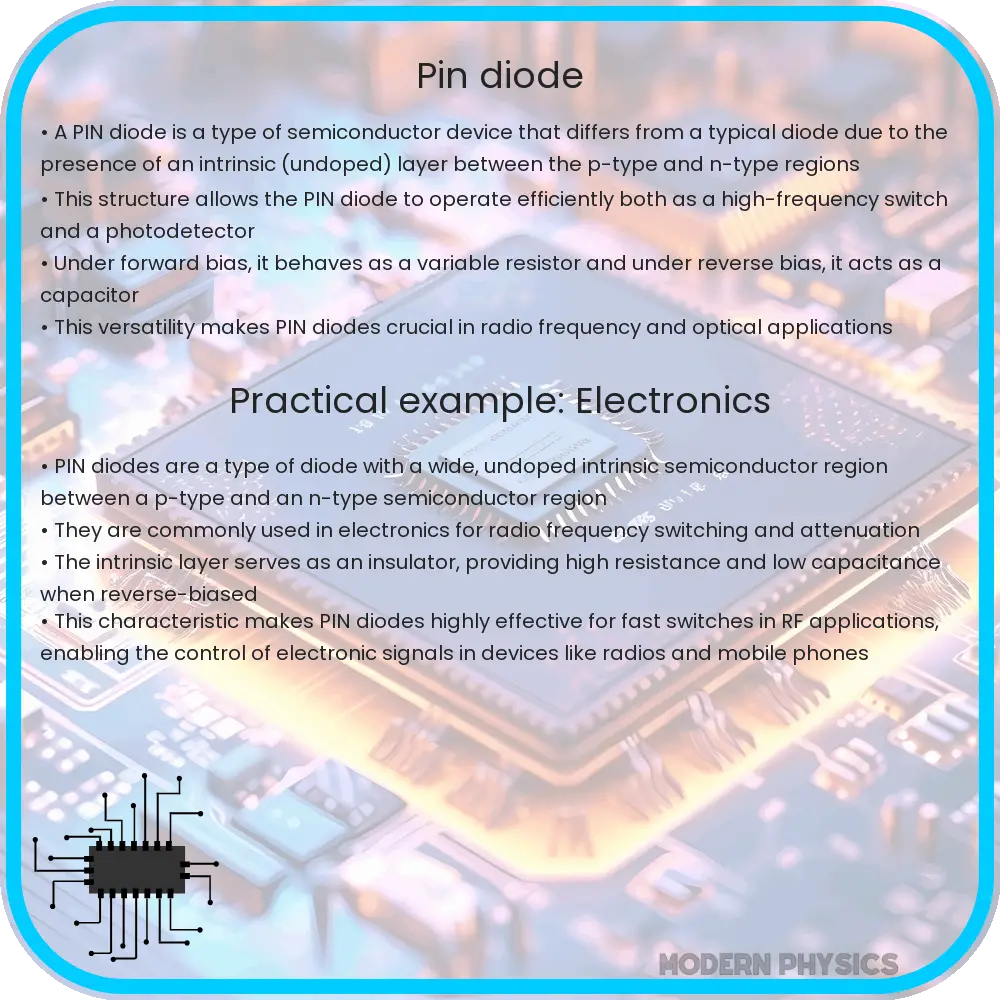
Learn about the PIN diode, a semiconductor with a unique layer structure enabling fast switching and efficient performance in RF applications.

Understanding the PIN Diode: Characteristics and Applications
A PIN diode is a type of semiconductor device that differs from a typical diode in its structure. It includes an intrinsic (I) layer sandwiched between a p-type and an n-type semiconductor. This intrinsic layer is crucial as it significantly changes the diode’s properties, enabling it to perform efficiently in various applications, including fast switching and RF (Radio Frequency) device roles.
Structure and Operation
The basic structure of a PIN diode consists of three layers: a P-type layer, an Intrinsic layer, and an N-type layer. The intrinsic layer between the P and N layers is undoped or very lightly doped, making it resistant to carrying current under normal conditions. When a forward bias is applied (positive voltage at P-side and negative at N-side), charge carriers (holes and electrons) inject from the P and N layers, respectively into the I layer. This charge accumulation leads to the reduction of the electric field within the I layer, allowing for an increased current flow through the diode.
Conversely, under reverse bias, the intrinsic layer widens and the diode switches to a high impedance state, significantly reducing the current flow. This ability to switch between a low and high impedance state makes the PIN diode incredibly valuable in RF and microwave switching and attenuations tasks.
Key Features of PIN Diodes
- Fast Switching: The thin intrinsic layer in PIN diodes allows for quick charge and discharge, enabling fast switching speeds essential in RF applications.
- Low Capacitance: Due to the wide intrinsic region, PIN diodes exhibit lower capacitance compared to regular PN junction diodes. This low capacitance is beneficial in high-frequency applications as it minimizes the distortion and attenuation of the signal.
- High Efficiency: In applications requiring high radiation tolerance, such as aerospace, the robust structure of PIN diodes makes them more efficient compared to other diodes.
Applications of PIN Diodes
PIN diodes are versatile and find applications across various sectors:
- RF Switches: The fast switching capability and low capacitance allow PIN diodes to be excellent components for RF switching, where they help alternate signal paths without introducing significant loss or distortion.
- Photodetectors: In optoelectronics, the intrinsic layer of PIN diodes can absorb light efficiently, making them suitable for use in photodetector circuits detecting wavelengths from infrared to ultraviolet.
- Attenuators: Their ability to operate under different bias conditions to control impedance makes PIN diodes effective for use in RF attenuators, adjusting signal strength during transmission or testing.
The versatility of PIN diodes is derived from their unique structure and electrical characteristics. By understanding these properties, engineers can deploy PIN diodes to optimize performance in specific applications, from telecommunications to power regulation systems. The next section will continue with the technical advantages of PIN diodes in modulating signal characteristics and ensuring system stability under varying operational conditions.
Technical Advantages in Signal Modulation
PIN diodes play a critical role in signal modulation, a process essential for effective communication systems. Due to their ability to change impedance rapidly under different electrical biases, these diodes can modulate amplitude, phase, and frequency of signals with high precision. This modulation capability is particularly advantageous in applications such as amplitude modulation (AM) transmitters or phase shift keying (PSK) systems used in data transmission.
Furthermore, the consistent performance of PIN diodes under high-frequency operations ensures reliable operation in environments subjected to rapid signal variations, thus maintaining the integrity of the communication channel.
Challenges and Limitations
While PIN diodes offer numerous benefits, they also come with challenges that need consideration:
- Power Handling: PIN diodes are typically not suited for very high-power applications. High power can lead to excessive heat generation within the diode, potentially damaging the device unless adequately managed.
- Reverse Recovery Time: Despite their fast switching capabilities, the intrinsic layer’s charge storage can lead to longer reverse recovery times compared to other diode types, which might not be ideal for extremely high-speed switching applications.
Engineers must carefully evaluate these limitations against the requirements of their specific applications to effectively utilize PIN diodes without compromising system performance.
Conclusion
PIN diodes are indispensable in the realm of modern electronics, providing specific advantages that are critical in areas ranging from RF switching to signal modulation. The unique structure of the PIN diode, characterized by its intrinsic layer, is the key to its versatile functionality in managing and manipulating electronic signals across various industries. Although they come with certain limitations, such as power handling and reverse recovery time, the benefits often outweigh these challenges, especially in specialized applications. Understanding and leveraging the properties of PIN diodes allow engineers to design more efficient and reliable electronic systems. By continuing to explore and innovate within this area, the capabilities and applications of PIN diodes can be expanded even further, paving the way for advanced technological developments.
