
Explore the transformative role of photonic crystals in waveguides, enhancing design efficiency, integration, and enabling advanced photonic devices.
Exploring the Role of Photonic Crystals in Waveguides: Enhancing Design Efficiency and Integration
Photonic crystals (PCs) have emerged as a cornerstone in the field of photonics, offering unparalleled control over the propagation of light. These materials are engineered to have periodic dielectric structures that affect the motion of photons in a similar manner to the way periodic potential affects electrons in a semiconductor. This capability not only enhances the efficiency of waveguides but also opens up new avenues for integration in photonic devices.
The essence of photonic crystals in waveguide design lies in their unique ability to manipulate the photonic band gap. This property allows for the selective transmission or reflection of light waves, enabling the creation of highly efficient waveguides with tailored dispersion properties. By incorporating PCs into waveguide designs, engineers can achieve precise control over light propagation, leading to significant improvements in signal transmission and overall device performance.
- Bandgap Engineering: The photonic band gap of PCs can be precisely controlled through the alteration of the periodic lattice structure. This enables the design of waveguides that can effectively guide light with minimal losses, even around tight bends.
- Integration with Other Photonic Devices: PCs in waveguides facilitate the seamless integration with other photonic components, such as lasers and modulators. This compatibility is crucial for the development of compact, integrated photonic circuits.
- Enhanced Light-Matter Interaction: The ability of PCs to localize light within a very small volume enhances the interaction between light and matter, which is beneficial for sensing applications and nonlinear optical devices.
The design and integration of photonic crystals in waveguides require meticulous attention to the interaction between light and the photonic crystal structure. Computational methods such as Finite-Difference Time-Domain (FDTD) and Plane Wave Expansion (PWE) are commonly employed to model and optimize these interactions. The objective is to tailor the photonic band gap and the defect states within the crystal to guide light efficiently through the waveguide.
In conclusion, the integration of photonic crystals into waveguide design represents a significant leap forward in the development of high-efficiency, integrated photonic devices. Through strategic manipulation of the photonic band gap and careful design considerations, engineers can harness the full potential of PCs to revolutionize the field of photonics.
Advancements and Challenges in Photonic Crystal Waveguide Integration
The integration of photonic crystals (PCs) into waveguides has marked a pivotal shift in optical communications, sensing technologies, and computational photonics. As research and development in this field advance, the potential applications of these materials continue to expand, promising a future where light can be manipulated with unprecedented precision and efficiency.
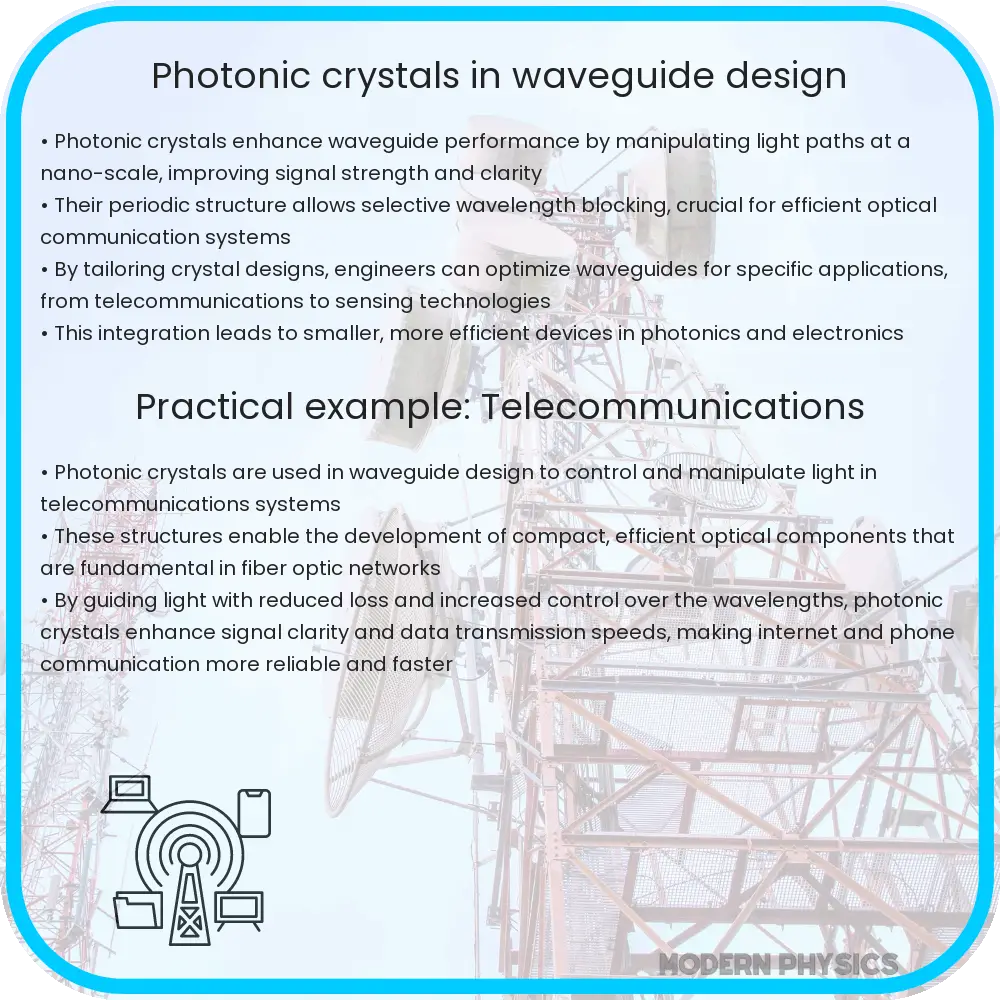
One of the most promising areas of development is in the realm of on-chip optical communications. Here, PCs offer a solution to the bandwidth and speed limitations of traditional electronic circuits. By enabling light to be tightly confined and directed with minimal loss, PCs integrated into waveguides can significantly enhance the data transmission capabilities of optical chips, making them ideal for future computing and telecommunications infrastructure.
Additionally, the sensitivity of photonic crystal waveguides to changes in their environment makes them excellent candidates for bio-sensing and environmental monitoring applications. The ability to detect minute changes in refractive index can be harnessed to create sensors capable of identifying single molecules, potentially revolutionizing medical diagnostics and environmental science.
- Scalability: As the demand for more compact and efficient photonic devices grows, scaling down photonic crystal waveguides while maintaining their performance remains a challenge. Advances in nanofabrication techniques are critical to overcoming this hurdle.
- Material Innovation: Exploring new materials and optimizing existing ones for photonic crystal fabrication can lead to waveguides with better optical properties and compatibility with other photonic components.
- Integration Complexity: The complexity of integrating PCs with other photonic and electronic components in a single device requires innovative design and fabrication approaches to ensure seamless operation.
In conclusion, photonic crystals in waveguides represent a transformative technology in the field of photonics, offering unprecedented control over light propagation. Their integration into waveguide designs not only enhances efficiency and performance but also opens up new possibilities for compact, integrated photonic circuits. Despite the challenges in scalability, material innovation, and integration complexity, ongoing research and technological advancements are paving the way for a future dominated by sophisticated photonic devices. The promise of PCs in enhancing communication, computation, and sensing technologies is immense, heralding a new era in the manipulation of light.