
Explore the revolutionary world of nanophotonic waveguides, their efficient design, advanced applications, and future impact on technology.
Understanding Nanophotonic Waveguides: Pioneering the Future of Miniaturized Technology
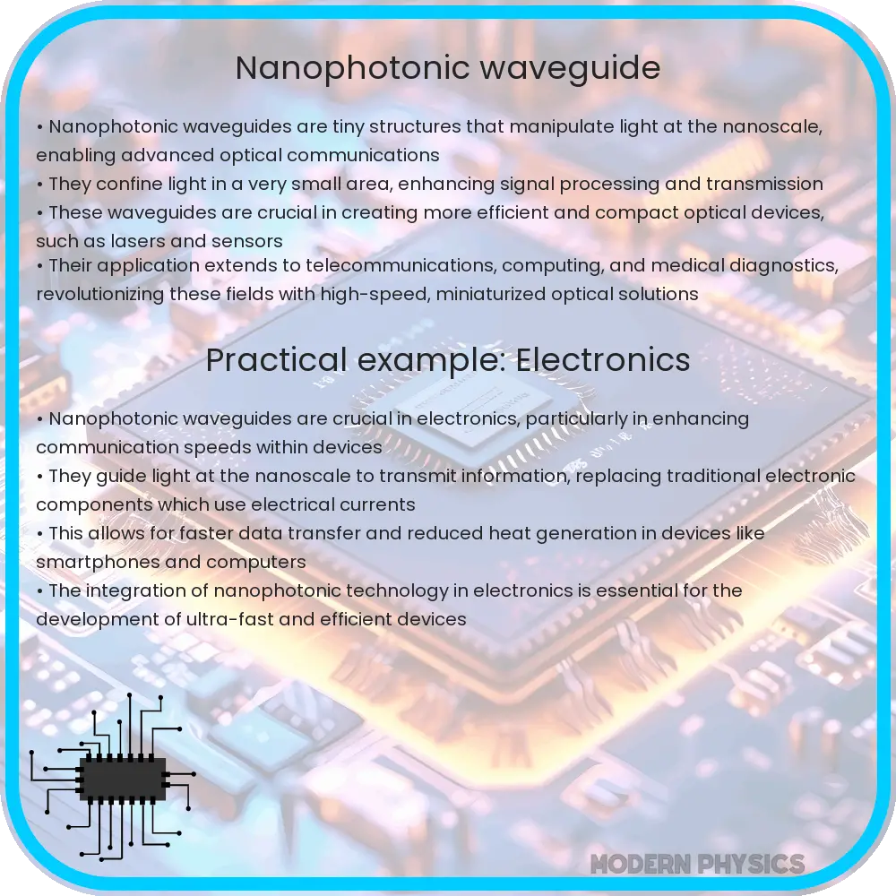
Nanophotonic waveguides represent a significant advancement in the field of optical technology. These microscopic structures guide light at the nanoscale, enabling unprecedented control over light propagation. This technological breakthrough is crucial for a variety of applications, from high-speed data transmission to sensitive biochemical sensing. In this article, we delve into the fundamentals of nanophotonic waveguides, their efficient design principles, and the promising future they hold.
Basics of Nanophotonic Waveguides
At its core, a nanophotonic waveguide is a structure that confines and directs light on a scale typically less than the wavelength of light itself. This confinement is achieved using materials with different refractive indices. The key to their efficiency lies in the precision of their design, which allows light to be guided with minimal loss.
Efficient Design and Miniaturization
The miniaturization of these waveguides is a technological marvel. Traditional optical fibers, although efficient, are bulky and inflexible, limiting their application in compact devices. Nanophotonic waveguides, on the other hand, are incredibly small – often just a few hundred nanometers in width. This small size enables their integration into a variety of devices, from tiny sensors to compact communication systems. The design of these waveguides often involves complex materials like silicon (Si), silicon nitride (Si3N4), and gallium arsenide (GaAs), which are known for their excellent optical properties.
Advanced Applications and Future Prospects
Nanophotonic waveguides are not just a theoretical concept but have practical applications that are reshaping technology. In telecommunications, they promise to dramatically increase the bandwidth and speed of data transmission. In the field of biosensing, they can detect minute changes in chemical compositions, making them invaluable for medical diagnostics and environmental monitoring.
Furthermore, these waveguides are paving the way for the development of highly efficient photonic integrated circuits (PICs). PICs combine multiple photonic functions on a single chip, analogous to how electronic integrated circuits revolutionized electronics. This integration could lead to more compact, efficient, and faster optical devices, essential for future computing and communication technologies.
The advancement of nanophotonic waveguides also opens the door to quantum computing applications. By manipulating photons at the nanoscale, these waveguides could play a crucial role in the development of quantum communication systems, offering unparalleled security and speed.
In conclusion, nanophotonic waveguides represent a significant leap forward in optical technology. Their efficient, miniaturized design and advanced applications herald a new era of integrated, fast, and compact devices, with wide-ranging implications across multiple industries.
Challenges and Innovations
Despite their numerous advantages, the development of nanophotonic waveguides is not without challenges. One of the primary difficulties lies in the precise fabrication of these tiny structures. The intricate patterns required for effective light guidance demand advanced lithography techniques and meticulous material processing. Additionally, as these waveguides shrink in size, they become more susceptible to external disturbances like temperature fluctuations and mechanical stress, which can affect their performance.
However, these challenges have not dampened the enthusiasm of researchers and engineers. Innovations in materials science and fabrication techniques are continually being developed to overcome these obstacles. For instance, new materials with lower refractive indices and improved thermal stability are being investigated. Likewise, advanced lithography methods are being refined to achieve more precise and efficient waveguide structures.
The integration of nanophotonic waveguides with electronic components is another area of ongoing research. This integration is crucial for developing fully functional photonic devices that can operate seamlessly with existing electronic systems. Efforts are being made to develop efficient methods for coupling light into and out of these waveguides, which is essential for their practical application.
In summary, while nanophotonic waveguides face certain fabrication and integration challenges, the field is rapidly advancing with new materials and techniques. These innovations are setting the stage for a new generation of optical devices that are more efficient, compact, and versatile than ever before.
Environmental Impact and Sustainability
As we embrace the potential of nanophotonic waveguides, it’s also crucial to consider their environmental impact. The production of these devices involves sophisticated manufacturing processes, which can have ecological footprints
. It’s essential to develop sustainable manufacturing practices and use environmentally friendly materials. Efforts are underway to reduce waste and energy consumption during production, ensuring that nanophotonic technologies contribute positively to environmental sustainability.
In addition to manufacturing concerns, the long-term operation and disposal of nanophotonic devices also pose environmental challenges. Research is focused on developing waveguides with longer lifespans and recyclable components. By enhancing the durability and recyclability of these devices, the environmental impact can be significantly minimized.
Moreover, the energy-efficient nature of nanophotonic waveguides offers a sustainable alternative to traditional optical technologies. Their minimal energy requirements for data transmission and processing can lead to a substantial reduction in overall energy consumption in communication networks and computing systems. This efficiency is not only beneficial for reducing operational costs but also for minimizing carbon footprints.
In conclusion, while nanophotonic waveguides present revolutionary technological advancements, their development and application must be guided by principles of sustainability and environmental responsibility. Ongoing research and innovation in sustainable materials, efficient manufacturing processes, and energy-efficient designs are critical for ensuring that this technology contributes positively to a sustainable future.
Final Thoughts
Nanophotonic waveguides represent a pivotal development in optical technology, offering efficient, miniaturized, and advanced solutions for a myriad of applications. From high-speed data transmission to quantum computing, they are setting new benchmarks in performance and integration. While challenges in fabrication and environmental impact remain, continuous advancements in materials science and manufacturing techniques are paving the way for their widespread adoption. As we move forward, the focus on sustainability will ensure that these innovations not only advance technological capabilities but also contribute to a more environmentally conscious world.
As we continue to explore the possibilities of nanophotonic waveguides, their role in shaping the future of technology becomes increasingly evident. Their potential to revolutionize communication, computing, and sensing technologies is immense, promising a future where miniaturized, efficient, and advanced optical devices are an integral part of our daily lives.
Stay tuned for further developments in this exciting field as researchers and engineers work towards harnessing the full potential of nanophotonic waveguides, driving innovation, and shaping the future of technology.
Expanding Horizons: The Future of Nanophotonic Waveguides
The realm of nanophotonic waveguides is not just limited to current applications. Future prospects are incredibly vast and diverse. Emerging fields like quantum computing and deep-space communication are poised to benefit significantly from the advancements in nanophotonic technologies. As researchers continue to unravel the intricacies of light manipulation at the nanoscale, new horizons in both fundamental science and practical applications are expected to emerge.
One of the most exciting areas of future exploration is the integration of nanophotonic waveguides with artificial intelligence (AI) and machine learning (ML). AI and ML can play a pivotal role in optimizing the design and functionality of these waveguides, leading to smarter, more adaptive optical systems. This synergy could revolutionize fields like autonomous vehicles, robotics, and smart cities, where efficient and fast data processing is crucial.
Conclusion
Nanophotonic waveguides represent a blend of cutting-edge science and practical engineering. They stand at the forefront of a new era in optical technology, characterized by miniaturization, efficiency, and advanced capabilities. Their development reflects a profound understanding of light-matter interaction at the nanoscale, and their applications span across telecommunications, biosensing, quantum computing, and beyond.
The journey of nanophotonic waveguides from theoretical concepts to real-world applications embodies the relentless pursuit of innovation. Despite the challenges in fabrication and environmental concerns, the progress in this field is a testament to human ingenuity and the relentless pursuit of knowledge. The integration of these technologies into various sectors will undoubtedly play a pivotal role in shaping the future of technology.
In conclusion, nanophotonic waveguides are not just a technological advancement; they are a beacon of the future, symbolizing the endless possibilities that arise when we push the boundaries of science and technology. As we continue to explore and harness their potential, nanophotonic waveguides are set to revolutionize the way we interact with and utilize light, paving the way for a brighter, more efficient, and interconnected world.
As we look to the future, the importance of sustainable development and environmental consciousness in the field of nanophotonics cannot be overstated. The balance between technological advancement and ecological responsibility will be crucial in ensuring that these innovations not only enhance our capabilities but also contribute positively to our planet and its future.
Thus, nanophotonic waveguides stand as a symbol of human progress, a testament to our ability to manipulate the fundamental aspects of nature for the betterment of society. Their continued development and integration into various fields will undoubtedly be a key driver of technological innovation in the decades to come.