
Optical profilometry is a precise, non-contact technique for creating detailed 3D maps and analyzing surface structures, vital for fields like semiconductor manufacturing and biomedical engineering.
Optical Profilometry: Precision, 3D Mapping & Surface Analysis
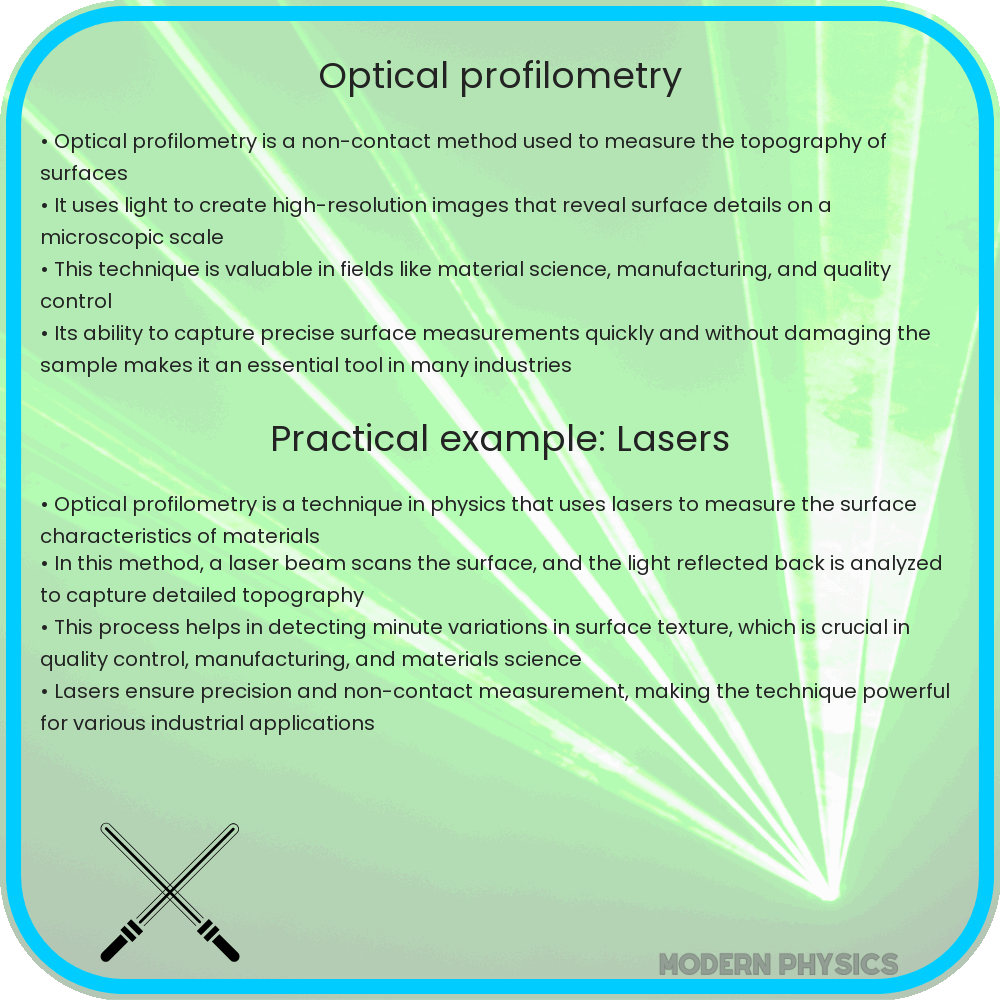
Optical profilometry is an advanced technique used for measuring the topography of surfaces with high precision. This non-contact method leverages light to obtain detailed 3D maps and analysis of surface structures, making it extremely valuable in various fields such as semiconductor manufacturing, materials science, and biomedical engineering.
How Optical Profilometry Works
At its core, optical profilometry uses light interference to create a detailed profile of a surface. Here’s a step-by-step breakdown of the basic principles behind this technique:
Precision and Accuracy
One of the key strengths of optical profilometry is its astounding precision. It can measure surface features down to the nanometer scale (1 nanometer = 1 x 10⁻⁹ meters). This high level of accuracy is achieved thanks to the principles of light interference and the sophisticated algorithms used in data processing. Several factors contribute to the precision of this method:
Applications of Optical Profilometry
Optical profilometry finds application across a variety of scientific and industrial domains:
In these applications, the ability to conduct non-contact, fast, and highly detailed surface measurements significantly enhances the efficiency and quality of production and research.
3D Mapping and Surface Analysis
The 3D maps generated by optical profilometry offer a comprehensive view of a surface’s texture, roughness, and other critical features. By using this data, engineers and scientists can:
The detailed 3D maps facilitate a better understanding of how surfaces interact with their environment, ultimately leading to improvements in design and manufacturing processes.
Advancements in Optical Profilometry
As technology has advanced, so has the field of optical profilometry. Modern systems come equipped with enhanced features that boost their capabilities:
Factors Affecting Measurement Quality
Despite the high precision of optical profilometry, several factors can impact the quality of measurements:
Conclusion
Optical profilometry has revolutionized the way we analyze and understand surface topography. Its ability to provide highly detailed 3D maps and precise measurements makes it an indispensable tool in semiconductor manufacturing, biomedical engineering, materials science, and many other fields. By leveraging light interference, sophisticated detectors, and advanced data processing software, this technology offers unparalleled precision and speed, enabling scientists and engineers to push the boundaries of innovation.
The ongoing advancements in optical profilometry, such as the integration of multi-wavelength systems and AI, promise to further enhance its capabilities, making it even more versatile and efficient. As we continue to refine this technology and address challenges like surface properties and environmental conditions, optical profilometry will undoubtedly play a crucial role in shaping the future of surface analysis and quality control.
Whether it’s ensuring the flawless production of microchips or analyzing the wear patterns on medical implants, optical profilometry provides the critical insights needed to improve designs, understand material properties, and advance technological progress. By making this powerful tool more accessible and user-friendly, we can foster greater innovation and exploration in science and engineering for years to come.