
Learn about high-k dielectric materials, crucial in semiconductor manufacturing for enhancing device performance and efficiency by replacing traditional silicon dioxide.
Introduction to High-K Dielectric Materials
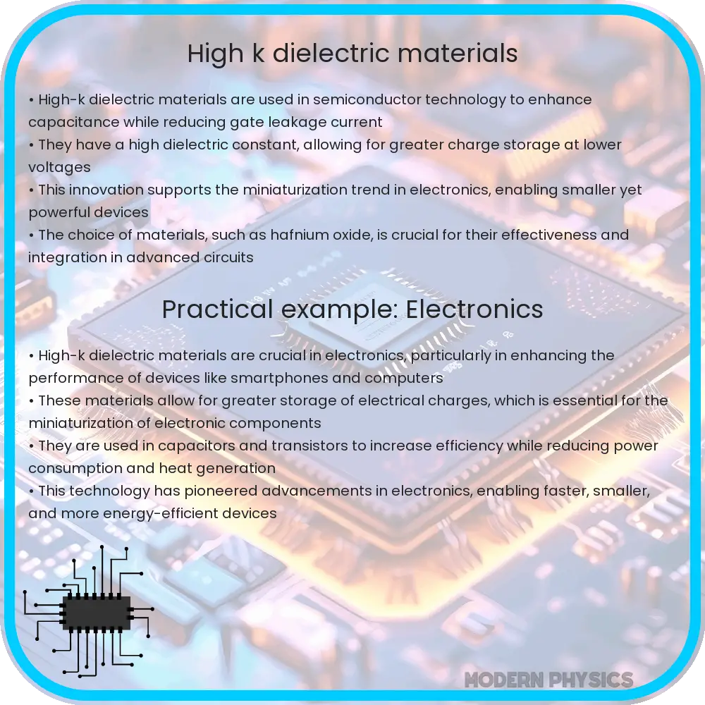
In the realm of semiconductor manufacturing, high-k dielectric materials have emerged as critical components, particularly for enhancing the performance and efficiency of modern electronic devices. These materials are primarily used as the gate dielectrics in metal-oxide-semiconductor field-effect transistors (MOSFETs). They replace the conventional silicon dioxide and offer the advantage of allowing further miniaturization while mitigating leakage currents, thus boosting both device efficiency and stability.
What are High-K Dielectrics?
A dielectric material is termed “high-k” if it has a high dielectric constant (k). The dielectric constant is a measure of a material’s ability to store electrical energy in an electric field. High-k dielectrics have a higher dielectric constant than silicon dioxide, which has been the traditional choice in semiconductor technologies. By implementing high-k materials, manufacturers are able to significantly reduce the thickness of the gate dielectric without increasing leakage currents, a common issue with thinner silicon dioxide layers in smaller devices.
Benefits of High-K Dielectrics
- Enhanced Capacitance: A higher dielectric constant allows for greater capacitance at the same thickness. This means that high-k materials can achieve the same capacitance values as thicker layers of traditional materials, leading to more compact and efficient designs.
- Reduced Power Consumption: Minimizing leakage currents means that devices using high-k materials use less power, which is vital for battery-operated devices like smartphones and laptops.
- Improved Reliability: These materials are also less prone to issues like electron tunnelling, which enhances the stability and reliability of the devices over time.
Challenges in Incorporating High-K Dielectrics
Despite their advantages, the integration of high-k dielectrics into semiconductor devices poses several challenges:
- Material Compatibility: High-k materials must be compatible with the existing semiconductor processes and must adhere effectively to other materials used in transistor fabrication, like silicon and metal gates.
- Thermal Stability: These materials need to be stable at the high temperatures involved in semiconductor manufacturing processes.
- Uniformity and Consistency: Achieving uniform thin layers of high-k materials is critical for device performance and poses a significant challenge in terms of deposition techniques.
Efficiency and Stability of High-K Dielectrics
The efficiency and stability of high-k dielectric materials stem primarily from their electrical properties. The high dielectric constant allows for a thicker physical layer that significantly reduces direct tunneling leakage currents. This is particularly important as devices continue to shrink, and the demand for low power consumption increases.
The stability of these materials is influenced by their thermal and chemical properties. High-k dielectrics tend to have a robust structure that can withstand high temperatures, which is a crucial characteristic for materials used in high-performance environments.
Future Outlook of High-K Dielectric Materials
As technology continues to progress, the demand for smaller, faster, and more efficient electronic devices shows no sign of diminishing. This trend heralds a bright future for high-k dielectric materials in various applications beyond just MOSFETs. Researchers are exploring the use of high-k materials in capacitors, DRAM (Dynamic Random Access Memory), and even in some types of solar cells.
Moreover, ongoing research is directed towards discovering new high-k materials with even greater performance characteristics and overcoming current limitations in manufacturing processes. Innovations, such as atomic layer deposition (ALD), are enhancing the ability to layer these materials with atomic precision, which may solve many of the uniformity and consistency challenges currently faced.
Conclusion
In summary, high-k dielectric materials are revolutionizing the field of semiconductor manufacturing by enabling the development of smaller, more efficient, and more reliable electronic devices. Despite certain challenges like material compatibility and thermal stability, the advantages of high-k materials, such as increased capacitance and reduced power consumption, are invaluable. As research continues to advance, it is expected that these materials will feature more prominently not only in consumer electronics but also in other cutting-edge technologies. This progression promises to push the boundaries of what is currently possible in electronic device fabrication and performance.