
Explore the essentials of epitaxial growth in semiconductors: techniques, advantages, applications, and future trends shaping the electronics industry.
Understanding Epitaxial Growth in Semiconductors
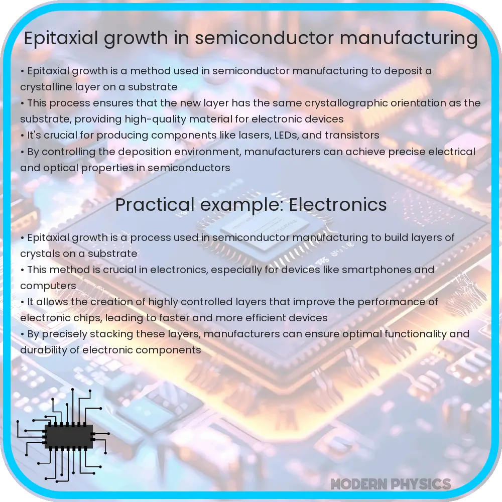
Epitaxial growth represents a cornerstone technique in the semiconductor industry, enabling the precise deposition of crystal layers on a monocrystalline substrate. This process is fundamental for the fabrication of advanced semiconductor devices, including transistors, lasers, and integrated circuits, which are integral to modern electronics. By aligning the crystallographic orientation of the grown layer with that of the substrate, epitaxial growth ensures high-quality materials characterized by exceptional electronic and optical properties.
The epitaxial process can be conducted through various methods, including Molecular Beam Epitaxy (MBE), Chemical Vapor Deposition (CVD), and Metal-Organic Chemical Vapor Deposition (MOCVD). Each technique offers unique advantages tailored to different materials and application requirements. MBE, for instance, excels in creating ultra-pure and well-defined layer structures, ideal for research and development settings. Conversely, CVD and MOCVD are favored in industrial applications for their higher throughput and versatility in depositing a wide range of materials, from silicon (Si) to complex compounds like gallium arsenide (GaAs).
Advantages of Epitaxial Growth
The precision of epitaxial growth enables the engineering of semiconductor properties at the atomic level, facilitating the design of devices with enhanced performance characteristics. For example, by adjusting the thickness, composition, and doping of epitaxial layers, manufacturers can create semiconductors with specific electrical, thermal, and optical properties. This level of control is crucial for developing high-speed, energy-efficient, and miniaturized components essential for today’s electronic devices.
Beyond device performance, epitaxial growth contributes significantly to the efficiency and cost-effectiveness of semiconductor manufacturing. By improving material quality and reducing defect densities, epitaxy enhances yield rates and device reliability, key factors for the economic production of semiconductors. Furthermore, the innovation driven by epitaxial techniques continues to push the boundaries of semiconductor technology, paving the way for future advancements in electronics and photonics.
In summary, epitaxial growth is an indispensable process in the semiconductor industry, marked by its precision, efficiency, and innovative potential. As we delve deeper into the mechanics and applications of epitaxy, it’s clear that this technique plays a pivotal role in shaping the landscape of modern electronics and beyond.
Mechanics and Applications of Epitaxial Growth
The mechanics of epitaxial growth involve complex interactions between the substrate and the deposited material. The process begins with the preparation of the substrate surface, which must be clean and free of defects to ensure the epitaxial layer grows correctly. During deposition, atoms or molecules from a gas or vapor phase condense on the substrate, aligning themselves to its crystal lattice in a process governed by surface kinetics and thermodynamics.
One of the critical factors in epitaxial growth is temperature control. The substrate temperature must be carefully regulated to balance between surface mobility and reactivity of the adsorbed species. This balance ensures that the deposited atoms have enough energy to move across the surface and find the correct lattice positions without desorbing or reacting prematurely.
Epitaxial growth finds applications in various fields beyond conventional semiconductors. In photonics, it is used to create laser diodes and LED structures that require precise control of light emission properties. In the realm of power electronics, epitaxial silicon carbide (SiC) layers are crucial for devices that operate at high temperatures, voltages, and frequencies. Moreover, epitaxy is instrumental in fabricating quantum dots and other nanostructures for quantum computing and advanced sensor technologies.
Challenges and Future Directions
Despite its numerous advantages, epitaxial growth faces challenges, including material quality, scalability, and cost. Defects such as dislocations and twin boundaries can degrade device performance, necessitating advanced characterization and quality control techniques. Additionally, the development of large-scale epitaxial growth processes that maintain high quality and uniformity remains a significant engineering challenge.
Future directions in epitaxial growth research focus on developing new materials, such as two-dimensional (2D) materials and heterostructures with unique electronic and optical properties. Innovations in growth techniques and equipment aim to improve scalability and reduce costs, making high-quality epitaxial layers more accessible for various applications.
Conclusion
Epitaxial growth is a fundamental process in semiconductor manufacturing, offering unparalleled precision in material fabrication. Its role extends beyond traditional electronics to emerging technologies in photonics, power electronics, and quantum computing. Despite challenges in material quality and process scalability, ongoing research and technological advancements continue to enhance its efficiency and applicability. As we push the boundaries of material science and engineering, epitaxial growth remains at the forefront, driving innovation and enabling the future of electronic and photonic devices.