
Learn about atomic lattice structures and their critical role in determining the properties of materials in physics and engineering.
Understanding Atomic Lattice: The Backbone of Material Science
The atomic lattice is a foundational concept in both physics and engineering, crucial for understanding the properties and behaviors of materials at the microscopic level. This structure is essentially a three-dimensional arrangement of atoms or molecules within a material, organized in a highly ordered pattern. These patterns not only define the bulk properties of the material but also influence their electrical, thermal, and mechanical characteristics.
Structure of Atomic Lattices
Atomic lattices are categorized primarily by the pattern in which their constituent particles are arranged. The most common lattice structures include face-centered cubic (FCC), body-centered cubic (BCC), and hexagonal close-packed (HCP). Each type of lattice has a distinct arrangement and coordination number, which significantly impacts the properties of the material.
- Face-Centered Cubic (FCC): In this structure, atoms are located at each of the corners and the centers of all the cube faces. Metals like aluminum, copper, and silver typically adopt this lattice structure.
- Body-Centered Cubic (BCC): BCC lattices have atoms at each corner of the cube and a single atom at the center of the cube. Examples include iron, chromium, and tungsten.
- Hexagonal Close-Packed (HCP): This structure features atoms at the corners of hexagons as well as additional atoms placed at hexagonal and triangular layers. Metals such as magnesium and zinc exhibit this type of lattice structure.
Properties Influenced by Atomic Lattices
The configuration of an atomic lattice plays a pivotal role in determining a material’s properties. This includes mechanical strength, electrical conductivity, and thermal expansion. For example, materials with a BCC lattice can usually withstand greater forces and are thus used in applications requiring high strength and durability.
- Electrical Conductivity: The arrangement of atoms in an FCC lattice often supports high electrical conductivity. This is because the densely packed arrangement allows electrons to flow more freely through the structure.
- Thermal Expansion: Atomic bonding and the lattice type dictate how much a material will expand or contract with temperature changes. Materials with BCC lattices, for instance, typically have higher rates of thermal expansion than those with FCC or HCP lattices.
Uses of Different Lattice Structured Materials
Understanding the differences in lattice structures is essential for various industrial and commercial applications. These materials can be tailored to specific needs based on their intrinsic lattice properties.
- Construction and Infrastructure: Steel, with its BCC structure, offers the high strength and durability required for building fronts and infrastructure projects like bridges and skyscrapers.
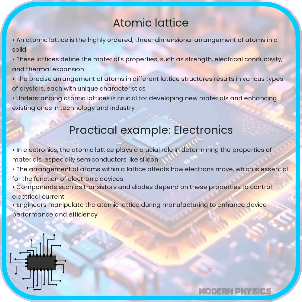
- Electronics: Materials with FCC lattice like copper and gold are extensively used in electrical wiring and electronic components due to their excellent conductivity.
- Aerospace: Titanium alloys, which often have an HCP structure, are favored in aerospace engineering for their strength-to-weight ratio and corrosion resistance.
Each lattice type brings different advantages to the materials that incorporate them, enabling engineers to choose the appropriate material based on the specific demands of their application. Understanding these structures allows for the innovative use of materials across different fields, pushing the boundaries of what is technologically possible.
Impact of Lattice Defects on Material Properties
While ideal atomic lattices offer theoretical insights into material properties, real-world materials often contain lattice defects. These imperfections, which include vacancies, interstitial atoms, and dislocations, can significantly affect the mechanical, thermal, and electronic properties of materials.
- Vacancies: These are essentially ‘missing’ atoms in the lattice and can lead to decreased strength and increased electrical resistivity.
- Interstitial Atoms: Atoms that are not part of the original lattice structure and are squeezed into interstitial spaces can distort the lattice, impacting the material’s properties.
- Dislocations: These are irregularities within the lattice that occur when layers of atoms are shifted. Dislocations are critical in determining the strength and plasticity of metals.
By manipulating these defects, engineers can tailor materials for specific uses, enhancing or mitigating certain properties to suit particular needs.
Advancements in Material Science
Recent advancements in technology have allowed scientists to manipulate atomic lattices with high precision, paving the way for the development of new materials with customized properties. Techniques such as crystal growth under controlled environments and the use of nanostructuring have contributed to significant improvements in material performance.
- Nanostructuring: This involves manipulating materials at the nanometer scale to achieve superior properties, such as increased strength or conductivity.
- Crystal Growth Technology: Advances in this area have enabled the production of very pure and defect-free crystals that are crucial for applications in electronics and optics.
Leveraging these techniques, engineers and scientists are continuously expanding the limits of materials, allowing for innovations in fields ranging from microelectronics to renewable energy systems.
Conclusion
The study of atomic lattice structures is more than an academic pursuit; it is a critical element of modern engineering and material science. By understanding the patterns and defects inherent in these structures, as well as leveraging technological advancements for precise manipulation, engineers can innovate and create materials that meet the evolving demands of industry and technology. This understanding not only helps in making informed choices about material usage but also drives forward the development of new applications that can transform our everyday lives. With each advancement in controlling and utilizing atomic lattices, we move closer to a future where material limitations are a thing of the past.