
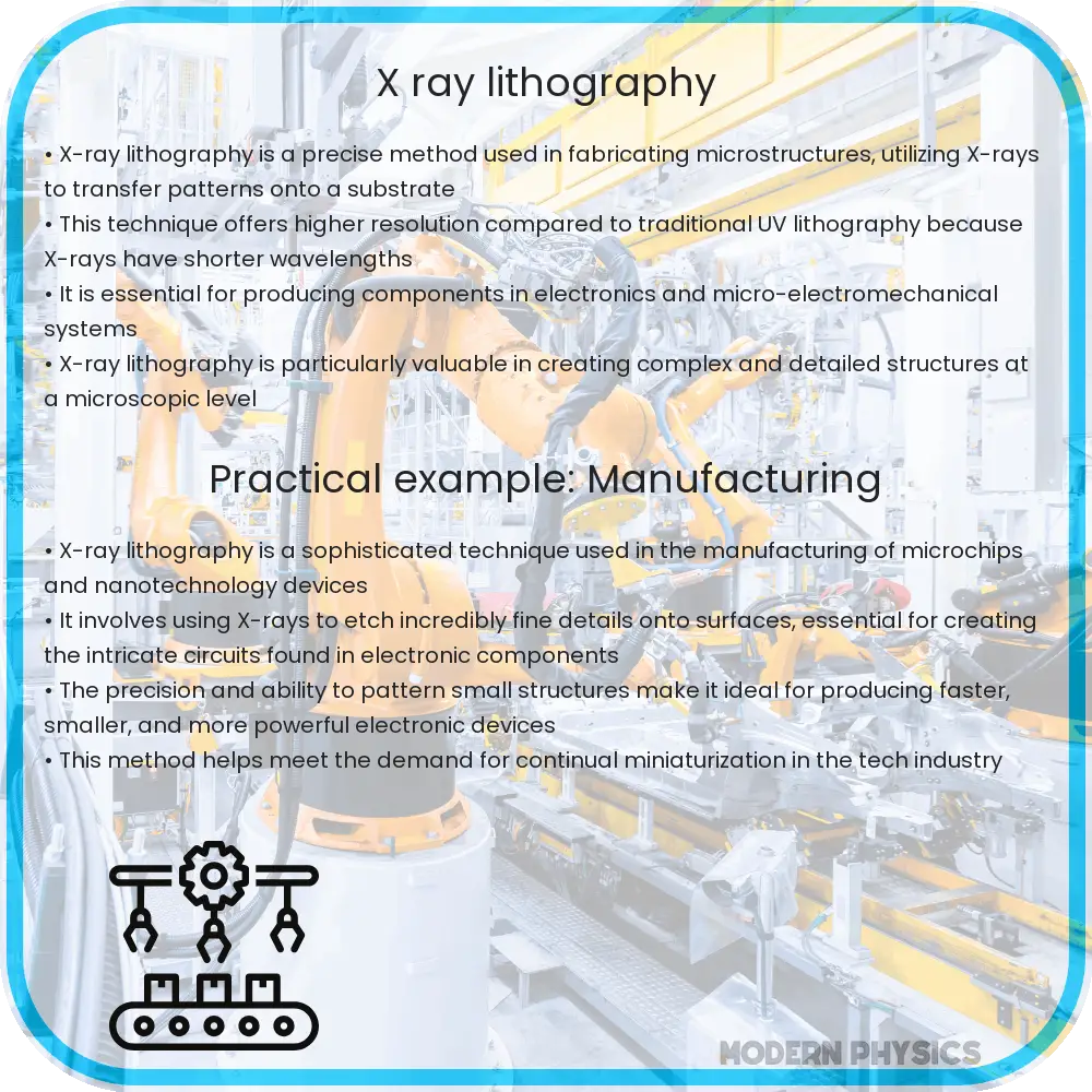
X-ray lithography is a microfabrication technique that uses X-rays for high-resolution patterning, essential in electronics, nanotechnology, and materials science.
X-ray Lithography: Precision, Scalability & Innovation in Materials Science
X-ray lithography represents a cutting-edge technique in the domain of microfabrication, playing a pivotal role in the advancement of numerous fields such as microelectronics, nanotechnology, and biomedical devices. This article delves into the essential aspects of X-ray lithography, including its remarkable precision, scalability, and how it fosters innovation in materials science.
Understanding X-ray Lithography
X-ray lithography is a process derived from photolithography, which itself is used extensively in the manufacturing of semiconductors. The primary difference between the two lies in the wavelength of light used to project patterns onto a substrate. While conventional photolithography employs ultraviolet light, X-ray lithography uses shorter wavelength X-rays. This fundamental difference makes X-ray lithography particularly valuable for its high resolution and ability to produce exceedingly small features, often on the order of nanometers.
Technical Insights of X-ray Lithography
The core principle behind X-ray lithography hinges on the use of X-rays to transfer a geometric pattern from a mask to a sensitive chemical photoresist on the substrate. Unlike optical lithography, X-ray lithography does not suffer from diffraction limits due to its shorter wavelengths, typically in the range of 0.1 to several nanometers. The process involves four main steps:
- Mask Creation: A mask is prepared with the desired pattern, made of a material opaque to X-rays, such as gold, on a thin membrane transparent to X-rays.
- Substrate Preparation: The substrate is coated with a photoresist that changes its properties upon exposure to X-rays.
- Exposure: The masked pattern is exposed to X-rays, which precisely imprint the mask’s pattern onto the photoresist.
- Development: After exposure, the substrate undergoes a development process, where the exposed or unexposed areas of the photoresist are washed away, depending on the type of resist used, leaving behind the desired patterned structure.
The equipment needed for X-ray lithography includes an X-ray source, which is typically a synchrotron radiation facility, providing powerful and stable X-rays. This source allows for consistent quality and high-precision in patterning.
Applications and Impact
X-ray lithography is instrumental in various applications due to its precision and ability to scale down. In electronics, it is used for creating high-density interconnects and capacitors necessary for the next generation of electronic devices. In the realm of materials science, it aids in producing nanoscale structures that can lead to new materials with enhanced properties, such as increased strength, lighter weight, or greater chemical resistance.
Moreover, its application in the development of micro-electro-mechanical systems (MEMS) and nano-electro-mechanical systems (NEMS) showcases its versatility and capacity to impact advanced engineering solutions. These systems, essential in creating tiny actuators, sensors, and motors, underscore X-ray lithography’s crucial role in miniaturization and technological progress.
The ability of X-ray lithography to scale complex patterns down to the nanometer level without losing precision allows for the exploration and development of new functionalities in materials, pushing the boundaries of what is achievable. This aspect is especially critical as industries strive towards the production of smaller, more efficient devices.
Challenges and Future Prospects
Despite its numerous advantages, X-ray lithography also faces certain challenges. One of the primary concerns is the cost and complexity of the equipment required, particularly the use of synchrotron radiation sources which are large and expensive. Additionally, the development of suitable masks and photoresists that can consistently perform under the intense energy of X-ray exposure remains a significant hurdle.
Looking to the future, advancements in compact X-ray sources and the development of more accessible technology could broaden the application of X-ray lithography. Researchers are also exploring alternative materials for masks and resist layers that are less costly and more environmentally friendly, which could help in reducing the overall cost of this technology.
Educational and Industrial Synergy
In educational settings, X-ray lithography offers a unique opportunity for students and researchers to engage directly with advanced manufacturing processes that are at the forefront of materials science. By integrating X-ray lithography projects into curriculum and research programs, educational institutions can foster an understanding of complex nanofabrication techniques and inspire innovation among the next generation of engineers and scientists.
Industrially, as the demand for miniaturized devices continues to grow, the role of X-ray lithography in manufacturing processes will likely expand. Industries ranging from electronics to biotechnology can benefit from the high precision and scalability of this technique. Ongoing collaboration between academic researchers and industry professionals is crucial to overcome current limitations and drive the future development of X-ray lithography technologies.
Conclusion
X-ray lithography stands out as a transformative technology in the field of microfabrication, marked by its exceptional precision and the ability to scale patterns to nanometer dimensions. While there are challenges in terms of equipment cost and materials development, the potential applications and impact of this technology continue to grow. It holds a crucial position in advancing microelectronics, MEMS, NEMS, and new materials science, shaping the future of various industries.
Encapsulating both the complexity and promise of this advanced technique, X-ray lithography not only pushes the boundaries of current engineering and scientific practices but also spurs continuous innovation and improvement. As technological and material advancements progress, X-ray lithography is poised to remain a key driver in the ongoing miniaturization and enhancement of electronic devices and systems. By overcoming existing hurdles, this technology could lead to further breakthroughs in multiple domains, enhancing both the functionality and efficiency of next-generation devices.