
Explore how quantum well devices enhance efficiency, precision, and speed in semiconductor technology, revolutionizing computing and renewable energy.
Introduction to Quantum Well Devices
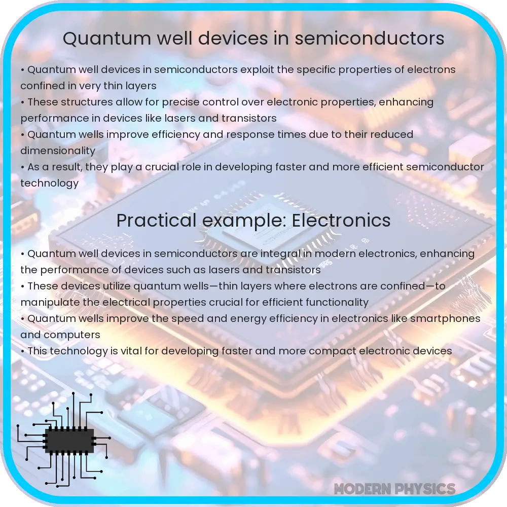
Quantum well devices represent a groundbreaking advancement in the realm of semiconductor technology, offering unparalleled improvements in efficiency, precision, and speed. By exploiting the principles of quantum mechanics, these devices achieve performance levels unattainable by conventional semiconductor components. This article delves into the fundamentals of quantum well devices, their operational mechanism, and their transformative impact on various technological sectors.
Understanding Quantum Wells
A quantum well is a potential well that confines particles, such as electrons or holes, in a dimensionally restricted space. It is typically formed when a thin layer of semiconductor material, with a narrow bandgap, is sandwiched between layers of a wider bandgap material. This configuration creates a well-like potential energy profile where charge carriers are confined in the narrow bandgap layer.
Enhanced Efficiency through Quantum Confinement
The quantum confinement effect within these wells leads to discrete energy states for the trapped particles, rather than the continuous states found in bulk materials. This quantization of energy states allows for more precise control over the electronic and optical properties of the device. As a result, quantum well devices exhibit significantly enhanced efficiency in light emission and absorption, making them ideal for applications in optoelectronics, such as lasers, light-emitting diodes (LEDs), and photodetectors.
Advancements in Precision and Speed
The ability to engineer the energy levels and band structures in quantum well devices enables unprecedented precision in device performance. This precision facilitates the development of high-speed electronic devices, including transistors and integrated circuits, capable of operating at frequencies and speeds beyond the reach of traditional semiconductor technologies. The reduced dimensionality and enhanced carrier mobility in quantum wells contribute to lower power consumption and faster response times, further amplifying their technological appeal.
Quantum well devices stand at the forefront of semiconductor innovation, offering a pathway to overcoming the physical limitations of conventional materials. Their application spans a wide range of fields, from telecommunications and computing to renewable energy and beyond, heralding a new era of efficiency, precision, and speed in electronic and optoelectronic devices.
Revolutionizing Telecommunications and Computing
The integration of quantum well devices into telecommunications infrastructure has led to the development of ultra-fast and efficient optical communication systems. Quantum well lasers, with their superior performance characteristics, enable high-speed data transmission over fiber-optic cables, drastically increasing the bandwidth and reliability of global communication networks. Similarly, in the computing realm, quantum well-based transistors and integrated circuits are paving the way for the next generation of high-performance processors. These processors promise not only higher speeds but also reduced energy consumption, addressing the critical need for sustainable and energy-efficient computing technologies.
Impact on Renewable Energy Technologies
Quantum well devices also play a pivotal role in enhancing the efficiency of renewable energy technologies. For instance, quantum well solar cells have demonstrated the ability to surpass the Shockley-Queisser limit, which is the theoretical maximum efficiency of traditional solar cells. By effectively harnessing the quantum confinement effect, these solar cells achieve higher absorption rates and convert a broader spectrum of sunlight into electricity, thereby significantly improving the efficiency and viability of solar power as a renewable energy source.
Challenges and Future Directions
Despite their numerous advantages, the widespread adoption of quantum well devices faces challenges. The complexity of their design and fabrication processes, coupled with the need for high-precision manufacturing techniques, currently limits their application and increases production costs. However, ongoing research and technological advancements are gradually overcoming these obstacles, making quantum well devices more accessible and cost-effective.
Future developments are expected to focus on further miniaturization, enhanced efficiency, and integration into a broader range of applications. Innovations in material science, nanotechnology, and quantum physics hold the key to unlocking the full potential of quantum well devices, potentially leading to breakthroughs in quantum computing, ultra-sensitive sensors, and next-generation electronic and photonic devices.
Conclusion
Quantum well devices represent a significant leap forward in semiconductor technology, offering enhanced efficiency, precision, and speed that far exceed the capabilities of traditional devices. By leveraging the unique properties of quantum mechanics, these devices have the potential to revolutionize telecommunications, computing, renewable energy, and many other sectors. Despite the challenges associated with their development and implementation, the ongoing advancements in this field promise to overcome these hurdles, paving the way for a future where quantum well technologies play a central role in driving innovation and progress across a wide array of technological landscapes.