
Explore the advancements in optical lithography equipment, focusing on precision, speed, and resolution crucial for next-gen semiconductor manufacturing.
Understanding Optical Lithography Equipment: A Deep Dive into Precision, Speed, and Resolution
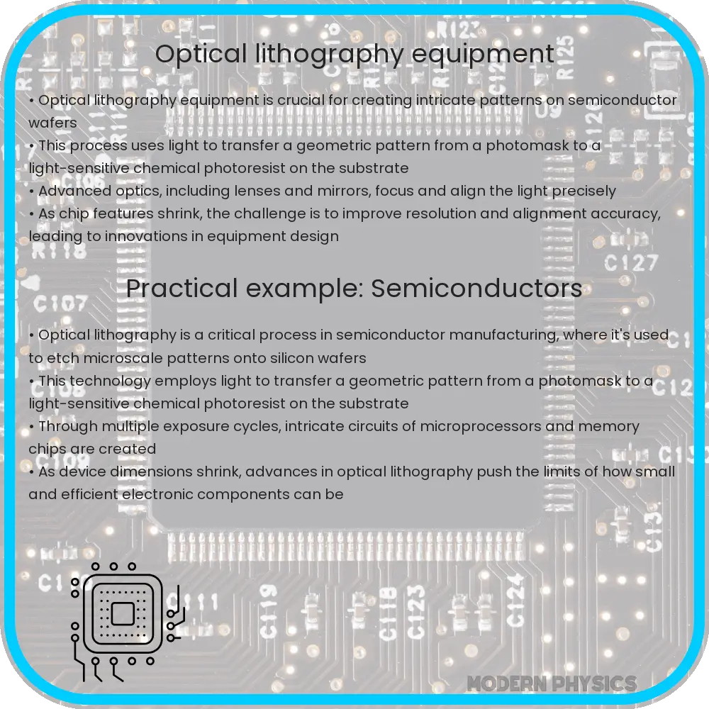
Optical lithography, a cornerstone technique in the semiconductor manufacturing process, plays a pivotal role in defining the pathways of electronic circuits on silicon wafers. This intricate process relies heavily on sophisticated equipment capable of manipulating light to etch micro and nano-scale patterns essential for integrated circuits (ICs). The precision, speed, and resolution of optical lithography equipment are critical factors that determine the efficiency and effectiveness of semiconductor fabrication, enabling the production of smaller, faster, and more efficient electronic devices.
Precision in Optical Lithography
The precision of optical lithography equipment is paramount, as it directly influences the accuracy of the patterns transferred onto the silicon substrate. This accuracy is crucial for minimizing defects and ensuring the functionality of the final semiconductor products. Advanced systems utilize ultraviolet (UV) light sources, such as deep ultraviolet (DUV) and extreme ultraviolet (EUV) lithography, to achieve higher precision. EUV lithography, for instance, employs a wavelength of approximately 13.5nm, allowing for the creation of features smaller than 7nm. The utilization of sophisticated optical components, including high-quality lenses and mirrors, further enhances the precision of these systems.
Speed Considerations
Speed is another vital attribute of optical lithography equipment, influencing the throughput and overall productivity of semiconductor manufacturing. The rapid pace at which these machines operate allows for the production of thousands of wafers per day. Equipment speed is a function of several factors, including the exposure time per wafer, the efficiency of the light source, and the automation level of the wafer handling system. Manufacturers continually seek advancements in light source intensity and system optimization to reduce cycle times and increase throughput.
Resolution: Pushing the Limits of Miniaturization
Resolution refers to the smallest feature size that optical lithography equipment can reliably print onto a wafer, a critical measure of its capability to produce next-generation semiconductor devices. The resolution is primarily determined by the wavelength of the light source and the optical system’s numerical aperture (NA). Techniques such as immersion lithography, where the space between the lens and the wafer is filled with a liquid with a high refractive index, have been developed to enhance resolution. This method effectively reduces the wavelength of the light in the medium, allowing for the printing of even finer features.
Is this conversation helpful so far?
The Evolution and Importance of Optical Lithography Equipment
Optical lithography has been a cornerstone in the semiconductor manufacturing industry, enabling the creation of intricate patterns on silicon wafers that form the basis of integrated circuits (ICs). As the demand for smaller, faster, and more efficient electronic devices grows, the precision, speed, and resolution of optical lithography equipment have become critical factors in the industry’s ability to keep pace with technological advancements.
Advancements in Precision and Resolution
The precision and resolution of optical lithography equipment have seen significant improvements over the years, thanks to advancements in light sources, photomasks, and optical systems. Modern lithography machines use deep ultraviolet (DUV) light sources, such as excimer lasers, to achieve feature sizes well below 100 nanometers (nm). The introduction of extreme ultraviolet (EUV) lithography has pushed the boundaries even further, enabling patterning below 10nm. These advancements are crucial for the production of next-generation chips required for applications such as artificial intelligence, 5G communications, and autonomous vehicles.
Enhancing Speed and Throughput
Speed and throughput are equally important in the semiconductor manufacturing process. The ability to expose patterns quickly and accurately over entire wafers is essential for meeting the high-volume production demands of the industry. To this end, optical lithography equipment manufacturers have focused on increasing the power of light sources and improving the efficiency of the exposure process. Stepper and scanner technologies have evolved to offer faster and more precise control over the lithography process, significantly increasing the number of wafers that can be processed per hour.
Conclusion
Optical lithography equipment has undergone remarkable evolution to meet the ever-increasing demands of the semiconductor industry. The advancements in precision, speed, and resolution are pivotal in the production of smaller, more complex ICs that power today’s electronic devices. As the industry continues to push the limits of Moore’s Law, the role of optical lithography in enabling future technological breakthroughs cannot be overstated. The ongoing developments in EUV lithography and other innovative technologies promise to further enhance the capabilities of optical lithography equipment, ensuring its critical position in semiconductor manufacturing for years to come.