
Explore how doping enhances semiconductor efficiency, conductivity, and control, including types of doping and their impact on device performance.
Understanding Doping in Semiconductors
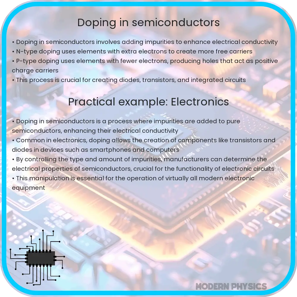
Doping, a fundamental process in semiconductor fabrication, significantly influences the efficiency, conductivity, and control of semiconductor devices. This method involves introducing impurities into an intrinsic (pure) semiconductor to modify its electrical properties. The choice of doping materials and the concentration of dopants are meticulously controlled to achieve desired electrical characteristics in semiconductors such as silicon (Si) or germanium (Ge).
Types of Doping
There are two main types of doping: n-type and p-type. N-type doping involves adding elements with more valence electrons than the semiconductor, typically from group V of the periodic table, such as phosphorus (P), arsenic (As), or antimony (Sb). This introduces extra electrons (negative charge carriers) into the semiconductor. The chemical notation for n-type doping in silicon would be Si:P, indicating phosphorus atoms have been added to the silicon lattice.
P-type doping, on the other hand, involves incorporating elements with fewer valence electrons, usually from group III, including boron (B), aluminum (Al), or gallium (Ga). This creates “holes” or positive charge carriers in the semiconductor. A p-type doped silicon could be denoted as Si:B, signifying the addition of boron atoms.
Efficiency and Conductivity Enhancement
Doping dramatically enhances the conductivity of semiconductors. By adding dopants, the number of charge carriers in the semiconductor increases, which directly improves its ability to conduct electricity. In solar cells, for example, the efficiency of light absorption and conversion into electrical energy is significantly boosted through doping. The introduction of p-n junctions, formed by adjoining p-type and n-type semiconductors, is crucial for creating diodes, transistors, and other semiconductor devices. These junctions allow for the controlled flow of electrons and holes, enabling the semiconductor device to perform its designated function efficiently.
Control over Semiconductor Properties
The level of doping can be precisely controlled to tailor the semiconductor’s properties for specific applications. For instance, high levels of doping can increase conductivity but may also introduce unwanted properties, such as increased noise in electronic signals. Therefore, achieving the right balance through doping is essential for optimizing the performance of semiconductor devices. Advanced fabrication techniques, including ion implantation and diffusion, allow for the precise introduction and distribution of dopants within the semiconductor lattice, providing engineers with the tools needed to design and manufacture high-performance semiconductor devices.
Advanced Applications of Doping
The strategic application of doping has paved the way for the development of cutting-edge semiconductor devices. High-frequency transistors, laser diodes, and light-emitting diodes (LEDs) are just a few examples where doping plays a crucial role. In high-frequency transistors, for instance, doping is used to create extremely thin layers of p-type and n-type materials, enabling these devices to operate at the gigahertz frequencies required for modern telecommunications. Similarly, the specific wavelengths of light emitted by LEDs are determined by the materials and doping levels used in their construction.
Challenges and Innovations in Doping Techniques
Despite its advantages, doping presents several challenges, including the need for precise control over dopant concentration and distribution. Unintended fluctuations in these areas can lead to significant variations in device performance. Moreover, as semiconductor devices continue to shrink in size, achieving uniform doping at the nanoscale becomes increasingly difficult. Innovations in doping techniques, such as molecular beam epitaxy (MBE) and chemical vapor deposition (CVD), have been instrumental in addressing these challenges. These methods allow for the controlled growth of doped semiconductor layers with atomic precision, essential for the fabrication of nanoscale devices.
Environmental and Safety Considerations
Environmental and safety concerns also accompany the doping process. Many dopants, such as arsenic, are toxic, and their handling and disposal require careful management to prevent environmental contamination and safeguard human health. The semiconductor industry has made significant strides in developing safer doping methods and materials, but the challenge of minimizing the environmental impact of semiconductor manufacturing remains.
Conclusion
The process of doping in semiconductors represents a cornerstone of modern electronics, enabling the development of devices that are integral to daily life, from smartphones to solar panels. By carefully introducing impurities into semiconductors, manufacturers can precisely control the electrical properties of these materials, enhancing efficiency, conductivity, and functionality. While challenges such as doping control at the nanoscale and environmental impact persist, ongoing innovations in doping techniques and materials continue to push the boundaries of semiconductor technology. As we look to the future, the role of doping in the evolution of semiconductor devices remains as vital as ever, promising new advancements in electronics and information technology.